Plasma coating systems for non-planar substrates

A plasma, non-planar technology, applied in the direction of ion implantation plating, metal material coating process, device for coating liquid on the surface, etc., can solve problems such as poor wear resistance

Active Publication Date: 2017-05-03
EXATEC LLC
View PDF17 Cites 0 Cited by
  • Summary
  • Abstract
  • Description
  • Claims
  • Application Information

AI Technical Summary

Problems solved by technology

But many plasma-deposited silicone coatings seem to degrade when exposed to UV, resulting in poor abrasion resistance

Method used


Image

  • Plasma coating systems for non-planar substrates
  • Plasma coating systems for non-planar substrates
  • Plasma coating systems for non-planar substrates

Examples


Embodiment 1

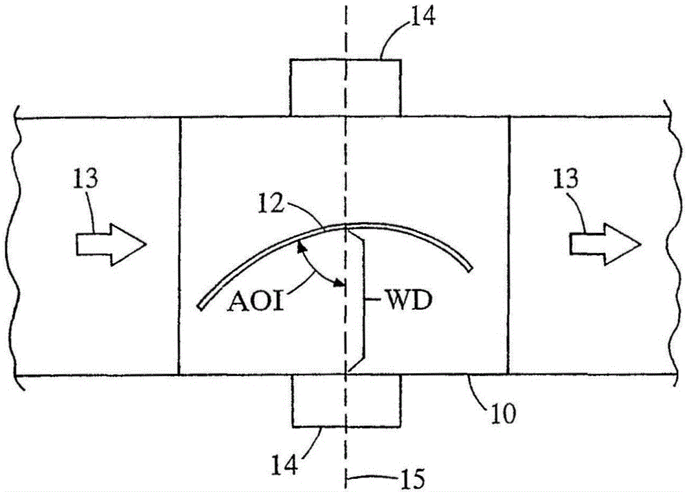
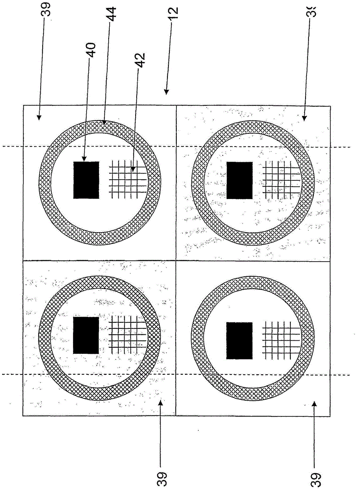
[0051] In this example, the MR10 sheets were coated with plasma polymerized and oxidized D4. During the coating process, the central lines of the two fixed ETP sources 14 are arranged parallel and separated by about 16 cm. This configuration is used to coat approximately 64in 2 Substrate. Mount four 4" x 4" sample 39 on aluminum fixtures such as figure 2 shown. Samples are indicated as 1T (top right), 1B (bottom right), 2T (top left) and 2B (bottom left). The substrate passed vertically past ETP source 14 at a scan speed of about 2.3 cm / sec. Rectangle 40 represents a typical location for a silicon chip. The coating thickness on these chips was determined by ellipsometry. During experiments in which coating thickness profiles were formed, silicon chips were placed every 1-inch along the substrate in vertical and horizontal lines. The cross-hatching 42 is at the position where the adhesion of the coating was measured before and after immersion in water at 65°C for 3 da...

Embodiment 2

[0055] The process conditions were similar to Example 1, except that the WD was increased to 31 cm. The final coating thickness was 2.1 microns, the same as Example 1, but the average Taber delta haze was increased to about 3% and about 4% (for both runs). Therefore, obtaining the desired coating thickness does not necessarily ensure good wear resistance of the coating, especially for coatings formed at larger WD. Therefore, non-planar parts with a WD exceeding the threshold WD do not have uniform wear resistance, even though the coating thickness may be uniform.

Embodiment 3

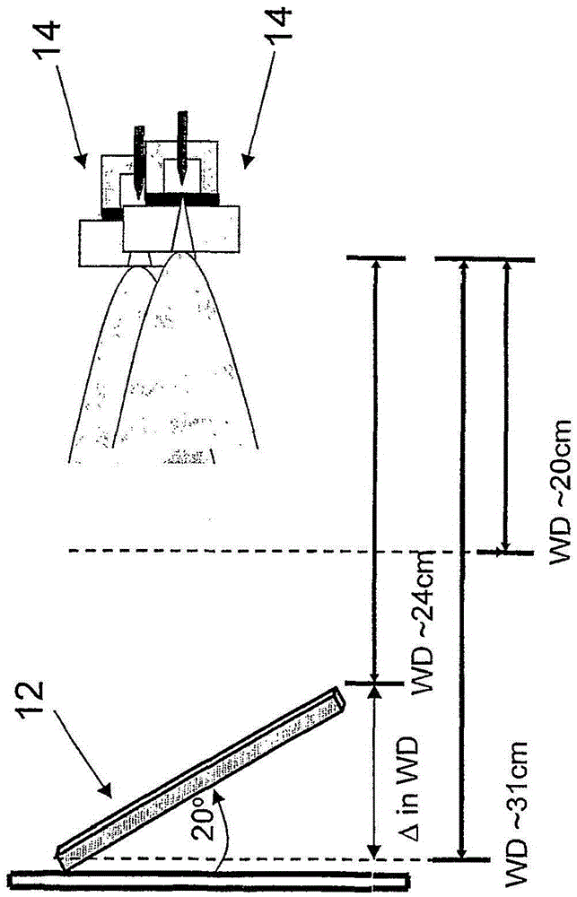
[0057] Process condition is similar to embodiment 1, but the angle of substrate holder is about 20 degrees (such as image 3 shown) such that the WD at the top of the substrate is 31 cm and the bottom is 24 cm. A uniform coating thickness of about 2.1 microns was obtained, but the Taber delta haze increased from about 4% at the bottom (ie, shorter working distance) to 10% at the top. Thus, Comparative Examples 1-3 show that flat or angled parts coated using these process conditions have poor Taber at relatively long working distances.


PUM

PropertyMeasurementUnit
thicknessaaaaaaaaaa
thicknessaaaaaaaaaa
thicknessaaaaaaaaaa

Abstract

A non-planar article comprising a plasma-deposited abrasion resistant coating having a substantially uniform thickness and a substantially uniform abrasion resistance with a delta haze (%) in the range of about + / -0.25 on average .

Description

[0001] This application is a divisional application of a Chinese patent application with the application number 200580012319.5, the filing date is March 8, 2005, and the invention title is "Plasma Coating System for Non-planar Substrates". [0002] related application [0003] This application claims the benefit of U.S. Provisional Application No. 60 / 551,931 (filed March 9, 2004, the entire contents of which are hereby incorporated by reference). technical field [0004] The present invention generally relates to an article and method for coating a substrate. More specifically, the present invention relates to a non-planar article having a plasma deposited abrasion resistant coating and a method for plasma coating a non-planar plastic substrate. Background technique [0005] Various techniques are used for the application of functional coatings to substrates. Traditionally chemical vapor deposition (CVD), and physical vapor deposition techniques such as sputtering and evap...

Claims


Application Information

Patent Timeline
Patent Type & Authority Patents(China)
IPC IPC(8): C23C16/513B05D5/06B05D7/24B32B9/04C08J7/18C23C14/02
CPCB05D1/62C23C16/513Y10T428/31663C23C16/50
Inventor B·A·科列瓦尔C·D·亚科万格洛T·米巴赫M·W·梅塞德斯
Owner EXATEC LLC
Why Eureka
Try Eureka