Semiconductor device and manufacturing method thereof
A manufacturing method and semiconductor technology, applied in semiconductor/solid-state device manufacturing, semiconductor devices, electrical components, etc., can solve problems such as performance that cannot meet actual needs, and achieve the effect of improving performance
- Summary
- Abstract
- Description
- Claims
- Application Information
AI Technical Summary
Problems solved by technology
Method used
Image

Examples
Embodiment 1
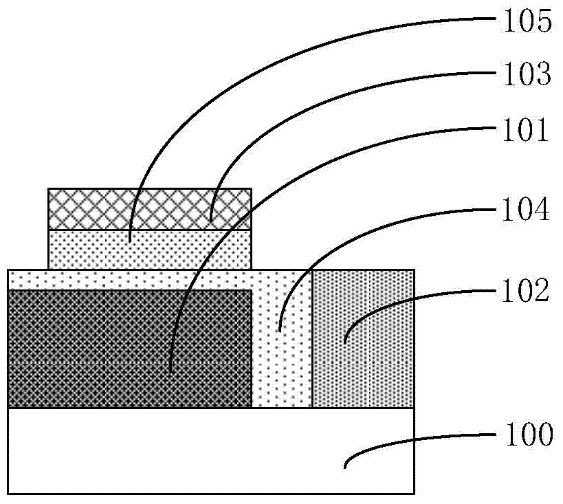
[0048] Below, refer to figure 2 The structure of the semiconductor device proposed by the embodiment of the present invention will be described, and the semiconductor device includes a new tunnel field effect transistor (TFET). in, figure 2 It is a schematic cross-sectional view of the structure of a semiconductor device according to an embodiment of the present invention.
[0049] This embodiment provides a new semiconductor device, which includes a TFET structure that can be compatible and integrated with a CMOS planar structure. The TFET is a high-performance TFET, wherein the TFET may be a vertical nanowire array TFET.
[0050] like figure 2 As shown, the semiconductor device of the embodiment of the present invention includes a semiconductor substrate 100 and an embedded insulating layer 1001 located in the semiconductor substrate 100 , and also includes a tunnel field effect transistor located on the semiconductor substrate 100 . Wherein, the tunnel field effect t...
Embodiment 2
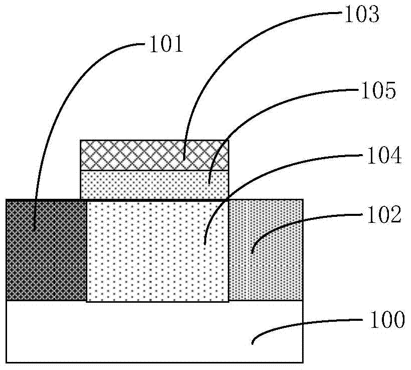
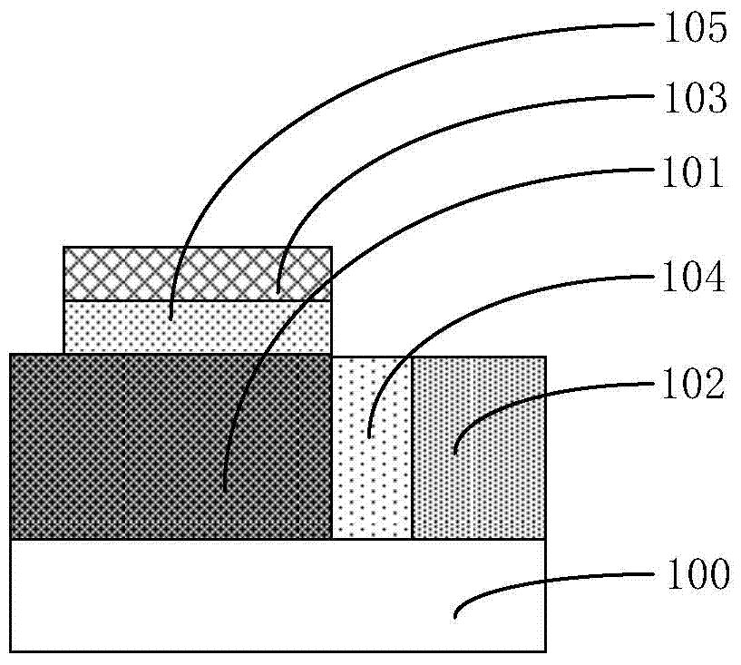
[0062] Below, refer to Figure 3A to Figure 3I and Figure 3D' , 3E’ as well as Figure 4 A method for manufacturing a semiconductor device proposed by an embodiment of the present invention will be described. in, Figure 3A to Figure 3I A schematic cross-sectional view of a pattern formed in some relevant steps of the method for manufacturing a semiconductor device according to an embodiment of the present invention; Figure 3D' for Figure 3D A top view of the graphics formed by the corresponding steps; Figure 3E' In the manufacturing method of the semiconductor device of the second embodiment of the present invention Figure 3E A top view of the graphics formed by the corresponding steps; Figure 4 It is a schematic flowchart of a method for manufacturing a semiconductor device according to an embodiment of the present invention.
[0063] The method for manufacturing a semiconductor device according to the embodiment of the present invention can be used to manufact...
PUM
| Property | Measurement | Unit |
|---|---|---|
| Doping concentration | aaaaa | aaaaa |
Abstract
Description
Claims
Application Information
 - Generate Ideas
- Intellectual Property
- Life Sciences
- Materials
- Tech Scout
- Unparalleled Data Quality
- Higher Quality Content
- 60% Fewer Hallucinations
Browse by: Latest US Patents, China's latest patents, Technical Efficacy Thesaurus, Application Domain, Technology Topic, Popular Technical Reports.
© 2025 PatSnap. All rights reserved.Legal|Privacy policy|Modern Slavery Act Transparency Statement|Sitemap|About US| Contact US: help@patsnap.com