Semiconductor device manufacturing method

A device manufacturing method and semiconductor technology, applied in semiconductor/solid-state device manufacturing, electrical components, circuits, etc., can solve the difficulty of increasing CMOS integration, the increasingly higher requirements for the thickness of metal gate stacks, and the difficulty of filling metal gate materials, etc. problem, to achieve the effect of multi-threshold voltage regulation, simplify the CMOS integration process, and reduce the effect of the reverse direction

Inactive Publication Date: 2015-07-08
INST OF MICROELECTRONICS CHINESE ACAD OF SCI
View PDF5 Cites 24 Cited by
  • Summary
  • Abstract
  • Description
  • Claims
  • Application Information

AI Technical Summary

Problems solved by technology

However, the choice of double metal gate material greatly increases the difficulty of CMOS integration, especially the gate stack filling holes prepared by the gate-last process are getting smaller and smaller, making it more and more difficult to fill the metal gate material, and the thickness of the metal gate stack The requirements are getting higher and higher

Method used


Image

  • Semiconductor device manufacturing method
  • Semiconductor device manufacturing method
  • Semiconductor device manufacturing method

Examples


Embodiment Construction

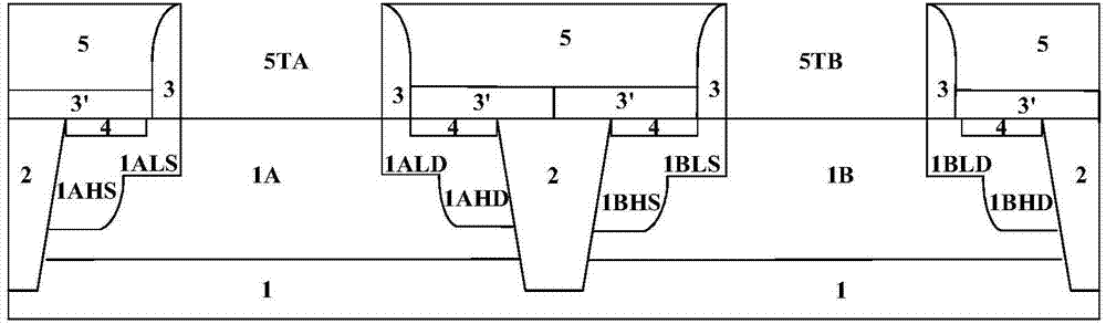
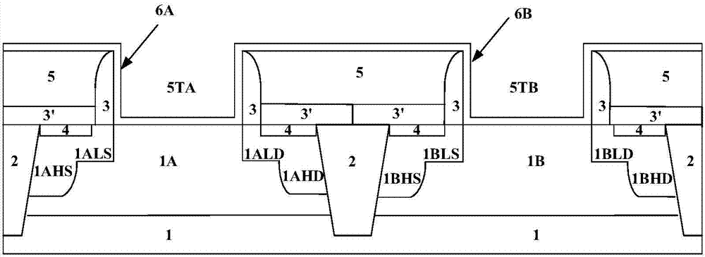
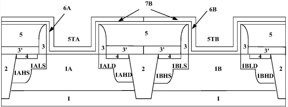
[0024] The features and technical effects of the technical solution of the present invention will be described in detail below with reference to the accompanying drawings and in conjunction with schematic embodiments, and a semiconductor device manufacturing method that simplifies the CMOS integration process and facilitates multi-threshold voltage regulation is disclosed. It should be pointed out that similar reference numerals represent similar structures, and the terms "first", "second", "upper", "lower" and the like used in this application can be used to modify various device structures or manufacturing processes . These modifications do not imply spatial, sequential or hierarchical relationships of the modified device structures or fabrication processes unless specifically stated.

[0025] In particular, in the following Figure 1 to Figure 7 In the cross-sectional view of , the left area represents the first active area that will eventually form an NFET, and the right a...


PUM


Abstract

The invention discloses a semiconductor device manufacturing method, which comprises steps: multiple first gate grooves and multiple second gate grooves are formed in a substrate; gate dielectric layers are formed in the multiple first gate grooves and the multiple second gate grooves; a second metal work function adjustment layer is formed on each gate dielectric layer; thicknesses of the second metal work function adjustment layers in the multiple first gate grooves are selectively adjusted; a first metal work function adjustment layer is formed on each second metal work function adjustment layer; a diffusion barrier layer is formed on the first metal work function adjustment layer; and a gate metal layer is formed on the diffusion barrier layer. According to the semiconductor device manufacturing method of the invention, through selectively depositing / etching the multiple metal work function layers on different device areas, the CMOS integrated technology is simplified, multi-threshold voltage regulation and control can be realized, and performance of the device is further improved.

Description

technical field [0001] The invention relates to a manufacturing method of a semiconductor device, in particular to a CMOS integration method of a semiconductor device. Background technique [0002] As the feature size of CMOS devices shrinks to the 22nm technology node and below, the material selection, preparation and equivalent work function adjustment of the metal gate stack structure of high-k gate dielectric / metal gate MOS devices are all technical difficulties. [0003] In order to meet the needs of the device, a double metal gate structure is generally used, that is: NMOFET uses materials with low metal work function such as titanium aluminum as the metal work function layer, and PMOSFET uses materials with high metal work function such as titanium nitride as the metal work function layer . However, the choice of double metal gate material greatly increases the difficulty of CMOS integration, especially the gate stack filling holes prepared by the gate-last process a...

Claims


Application Information

Patent Timeline
Patent Type & Authority Applications(China)
IPC IPC(8): H01L21/8238
CPCH01L21/8238
Inventor 杨红王文武赵超闫江殷华湘
Owner INST OF MICROELECTRONICS CHINESE ACAD OF SCI
Why Eureka
Try Eureka