
A full-wavelength localized plasmon resonance sensor and its preparation method

A resonant sensor and plasma technology, applied in the field of sensors, to achieve the effect of easy processing, high application value and low cost

Active Publication Date: 2018-06-01
SUN YAT SEN UNIV
View PDF6 Cites 0 Cited by
  • Summary
  • Abstract
  • Description
  • Claims
  • Application Information

AI Technical Summary

Problems solved by technology

[0005] The technical problem to be solved by the present invention is to overcome the defects of existing aluminum plasma materials, provide an aluminum nanomaterial substrate with localized plasma resonance peaks in the full wavelength range for sensing, and realize its uniform structure and large area manufacturing

Method used


Image

  • A full-wavelength localized plasmon resonance sensor and its preparation method
  • A full-wavelength localized plasmon resonance sensor and its preparation method
  • A full-wavelength localized plasmon resonance sensor and its preparation method

Examples


Embodiment 1

[0036] Example 1 Preparation of full-wavelength localized plasmon resonance sensor

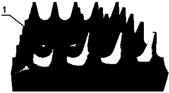
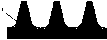
[0037] 1. attached Figure 1~2 A schematic diagram of a full-wavelength localized plasmon resonance sensor prepared for the present invention. The full-wavelength localized plasmon resonance sensor is characterized in that the sensor is an aluminum film whose surface structure is a nanocone array arranged periodically. The nanocones are formed by interlacing periodically arranged smooth depressions after the aluminum film is subjected to nanoimprinting and electrochemical etching.

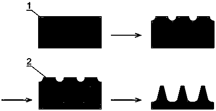
[0038] attached image 3 For the preparation process of the method of the present invention, the following detailed steps are included:

[0039] S1. Place the silicon template with periodic bumps on the surface of the clean and flat aluminum film in parallel, and apply a pressure of about 2×10 4 N / cm 2 , uniformly embossing nano pits;

[0040] S2. Connect the imprinted aluminum film on the electrochemical wor...

Embodiment 2

[0046] Example 2 Refractive index biosensing

[0047] Using the sensor of the present invention to detect the concentration of biochemical samples is achieved by comparing the baseline spectrum of the sensor with the spectrum cultivated by the sample to be tested, extracting the shift of the characteristic peak, and then calculating the concentration of the biochemical sample to be tested according to the calibration standard curve. The tumor marker CA199 in the serum of patients with colon cancer was selected for concentration detection, and all spectral measurements during the detection process were performed using Image 6 Measurement model.


PUM


Abstract

The invention discloses a full-wavelength local plasma resonance sensor and a preparation method thereof. The sensor is an aluminum nano-cone array, and the nano-cone array is formed by interlacing periodically arranged depressions on the surface of an aluminum sheet. The present invention can obtain different local surface plasmon resonance peaks in the full wavelength range by adjusting the incident angle, the three-dimensional size of the cone, and the size of the cone arrangement period, and can be applied to high-sensitivity refractive index sensing, Surface-enhanced fluorescence or surface-enhanced Raman scattering, etc. The invention has simple preparation technology, controllable structure, low cost and is suitable for large-scale production.

Description

technical field [0001] The invention belongs to the technical field of sensors. More specifically, it relates to a sensor with local plasmon resonance peaks in the full wavelength range of ultraviolet-visible-near-infrared light region and its preparation method. Background technique [0002] Metal nanoparticles or array substrates can match the incident light fluctuations with the surface plasmon waves without coupling prisms, optical waveguides or diffraction gratings. Under the incident light of a specific wavelength band, the surface plasmons can be stably excited and the incident light Localized in the region of subwavelength scale, this phenomenon is called localized plasmon resonance, which is widely used in the fields of refractive index sensing, surface-enhanced fluorescence, surface-enhanced Raman scattering, and nonlinear enhancement. So far, most of the research on localized surface plasmon sensing has focused on precious metal materials such as gold and silver....

Claims


Application Information

Patent Timeline
Patent Type & Authority Patents(China)
IPC IPC(8): G01N21/552
Inventor 周建华李万博江雪芹
Owner SUN YAT SEN UNIV
Learn More