Eureka AIR delivers breakthrough ideas for toughest innovation challenges, trusted by R&D personnel around the world.

Integrated circuit and metal interlayer dielectric layer planarization method

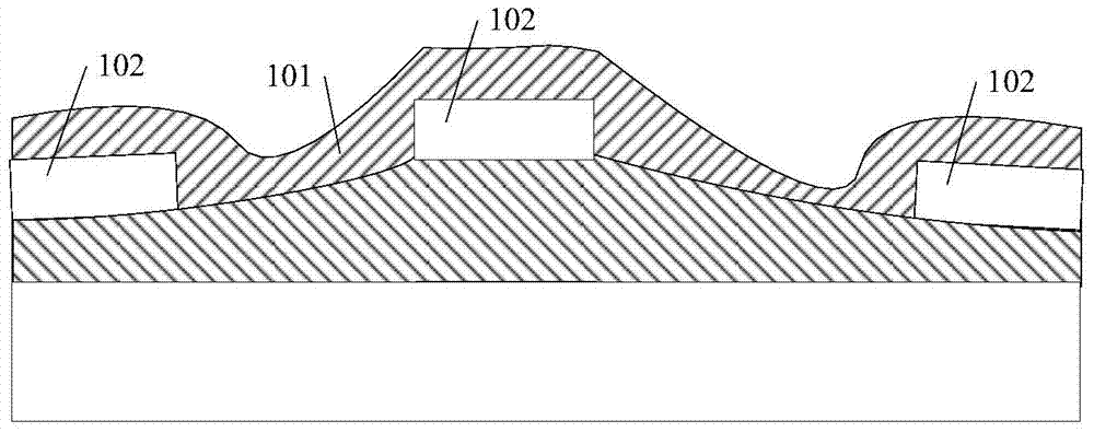
A technology of integrated circuits and metal layers, applied in the manufacture of circuits, electrical components, semiconductor/solid-state devices, etc., can solve the problems of poor surface planarization effect and affect the reliability of integrated circuits, and achieve the effect of improving the effect of planarization

Active Publication Date: 2015-07-15
FOUNDER MICROELECTRONICS INT
View PDF4 Cites 2 Cited by
  • Summary
  • Abstract
  • Description
  • Claims
  • Application Information

AI Technical Summary

Problems solved by technology

[0005] An embodiment of the present invention provides an integrated circuit and a method for planarizing an inter-metal dielectric layer thereof, so as to solve the problem in the prior art that the surface planarization effect of the inter-metal dielectric layer is poor and affects the reliability of the integrated circuit

Method used


Image

  • Integrated circuit and metal interlayer dielectric layer planarization method
  • Integrated circuit and metal interlayer dielectric layer planarization method
  • Integrated circuit and metal interlayer dielectric layer planarization method

Examples


Embodiment 1

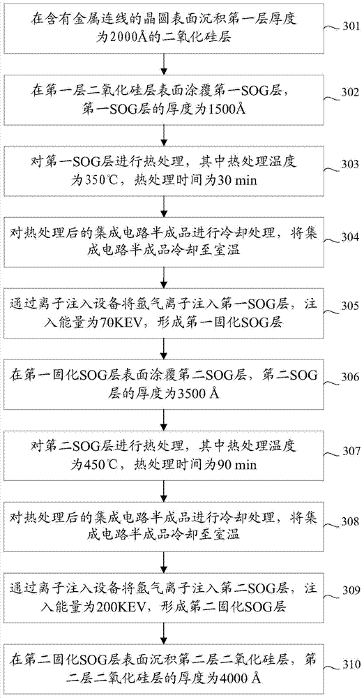
[0056] Such as image 3 As shown, it is Embodiment 1 of the method for planarizing the inter-metal dielectric layer of the integrated circuit in the embodiment of the present invention, and the method includes:

[0057] Step 301: Depositing a first layer with a thickness of The silicon dioxide layer; such as Figure 4 The schematic diagram of the structure after the first layer of silicon dioxide layer is deposited on the surface of the wafer in the embodiment of the present invention is shown, wherein 401 is the first layer of silicon dioxide layer, and 402 is a metal connection;

[0058] Step 302: Coating a first SOG layer on the surface of the first silicon dioxide layer, the thickness of the first SOG layer is

[0059] Step 303: performing heat treatment on the first SOG layer, wherein the heat treatment temperature is 350° C., and the heat treatment time is 30 minutes;

[0060] Step 304: cooling the semi-finished integrated circuit after heat treatment, and cooling ...

Embodiment 2

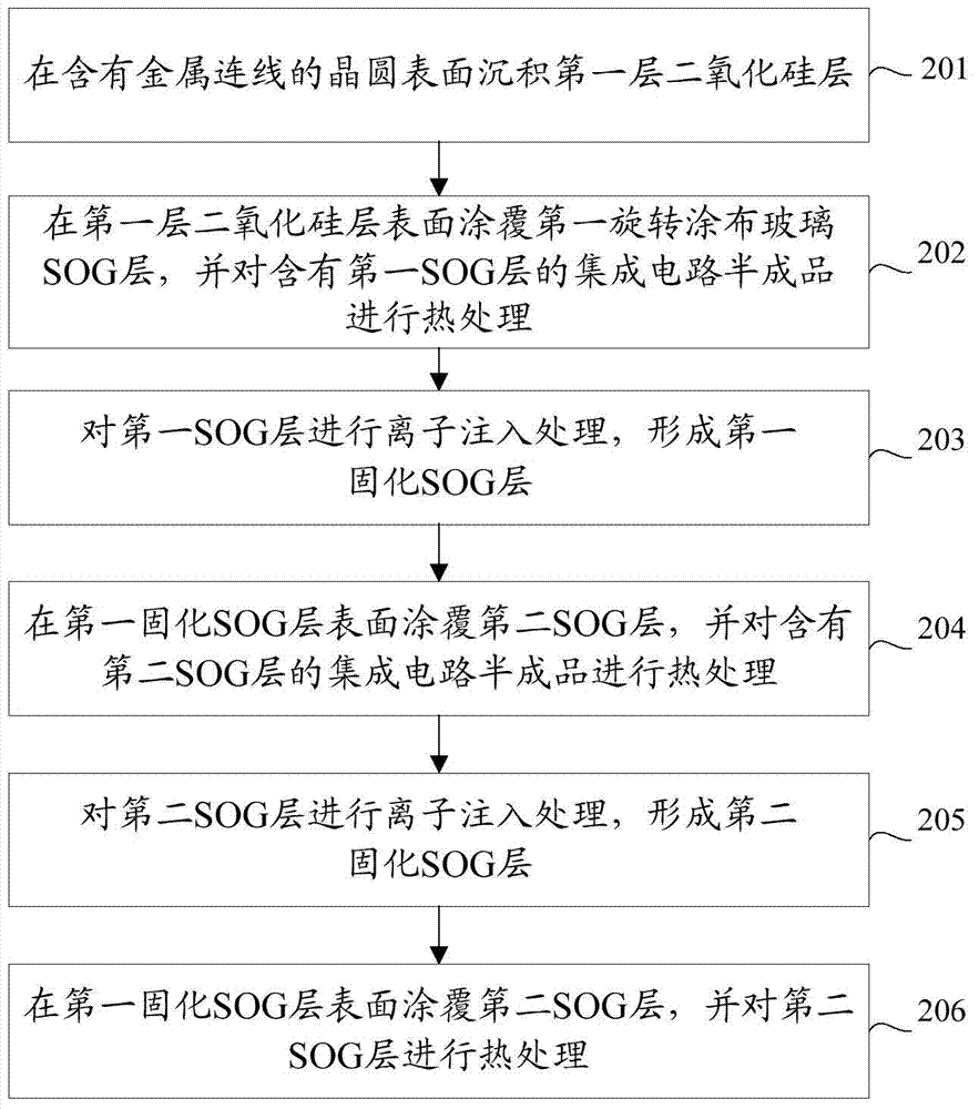
[0067] Such as Figure 8 As shown, it is the second embodiment of the method for planarizing the inter-metal dielectric layer of the integrated circuit in the embodiment of the present invention. The method includes:

[0068] Step 801: Depositing a first layer with a thickness of the silicon dioxide layer;

[0069] Step 802: Coating a first SOG layer on the surface of the first silicon dioxide layer, the thickness of the first SOG layer is

[0070] Step 803: performing heat treatment on the first SOG layer, wherein the heat treatment temperature is 375° C., and the heat treatment time is 45 minutes;

[0071] Step 804: cooling the semi-finished integrated circuit after heat treatment, cooling the semi-finished integrated circuit to room temperature;

[0072] Step 805: Implanting argon ions into the first SOG layer through ion implantation equipment with an implantation energy of 120KEV to form a first cured SOG layer;

[0073] Step 806: Coating a second SOG layer on the ...


PUM


Abstract

The embodiment of the invention relates to the field of semiconductor manufacturing, and particularly relates to an integrated circuit and a metal interlayer dielectric layer planarization method for the integrated circuit, so as to solve the problems that surface planarization effects of the metal interlayer dielectric layer are poor and reliability of the integrated circuit is influenced as etch-back is carried out on a spin coating glass layer in the prior art. According to the integrated circuit and the metal interlayer dielectric layer planarization method provided by the embodiment of the invention, as ion curing treatment is carried out on two SOG layers respectively, incomplete thickness curing of the two SOG layers can be avoided, and the integrated circuit can be prevented from having a broken layer; as etch-back treatment does not need to be carried out on the second SOG layer, the problem that the surface planarization degree of the metal interlayer dielectric layer is deteriorated as a result of different etch speeds, surface planarization effects of the metal interlayer dielectric layer are improved, and reliability of the integrated circuit is enhanced.

Description

technical field [0001] The invention relates to the field of semiconductor manufacturing, in particular to an integrated circuit and a method for planarizing a dielectric layer between metal layers thereof. Background technique [0002] In the manufacturing process of integrated circuits, the inter-metal dielectric layer is placed between the device and the interconnection metal layer as a protective layer to prevent the device from being polluted by impurity particles. As the feature size of CMOS (Complementary Metal Oxide Semiconductor, Complementary Metal Oxide Semiconductor) devices is getting smaller and smaller, the scale of integrated circuits is increasing rapidly, the number of layers of metal wiring is increasing, and the gap between metal wiring is getting narrower and narrower. , the planarization requirements for the inter-metal dielectric layer are also getting higher and higher. [0003] The method for the planarization of the metal interlayer dielectric laye...

Claims


Application Information

Patent Timeline
Patent Type & Authority Applications(China)
IPC IPC(8): H01L21/768
CPCH01L21/76819H01L21/76832
Inventor 张建湘王焜潘光燃文燕
Owner FOUNDER MICROELECTRONICS INT
Why Eureka
Eureka Blog
Learn More