MOS structure and method for making the same, and method for making metal silicide

A technology of metal silicide and MOS structure, which is applied in semiconductor/solid-state device manufacturing, semiconductor devices, electrical components, etc., can solve the problem of reducing gate resistance and contact resistance, the effect of reducing gate resistance and contact resistance is not very good, the resistance value is large, and the power consumption of semiconductor devices The effect is not very good and other problems, to achieve the effect of ensuring electrical performance, low power consumption, small grid resistance and contact resistance

Active Publication Date: 2018-05-01
FOUNDER MICROELECTRONICS INT
View PDF3 Cites 0 Cited by
  • Summary
  • Abstract
  • Description
  • Claims
  • Application Information

AI Technical Summary

Problems solved by technology

[0028] The embodiments of the present invention provide a MOS structure and its manufacturing method, as well as a method of manufacturing metal silicide in the MOS structure, which are used to solve the problem of metal silicide currently formed on the gate region, source region and drain region in the prior art. The resistance value of silicide is relatively large, so that the effect of reducing the gate resistance and contact resistance is not very good, resulting in the problem that the effect of reducing the power consumption of semiconductor devices including MOS structures is not very good.

Method used


Image

  • MOS structure and method for making the same, and method for making metal silicide
  • MOS structure and method for making the same, and method for making metal silicide
  • MOS structure and method for making the same, and method for making metal silicide

Examples


Embodiment 1

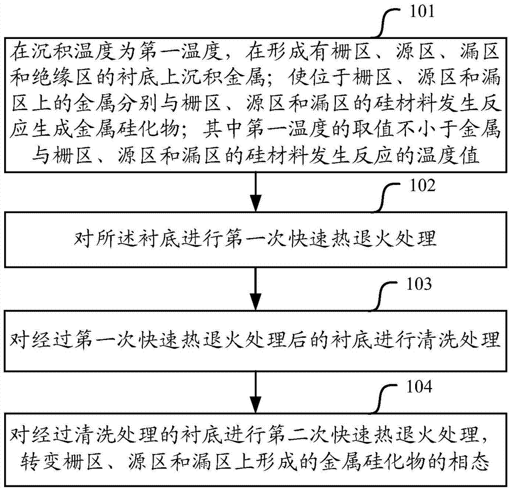
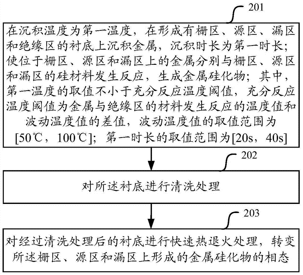
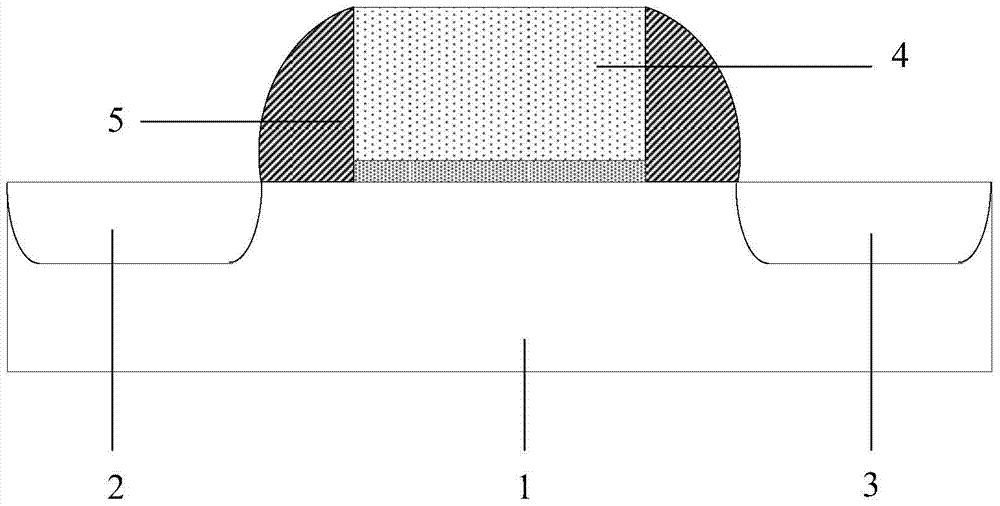
[0123] Such as Figure 3A As shown, the MOS structure includes a substrate 1, a source region 2 and a drain region 3 located in the substrate 1, and a gate region 4 and an insulating region 5 located on the substrate 1; wherein the materials of the source region 2 and the drain region 3 are Single crystal silicon, the material of the gate region 4 is polysilicon, and the material of the insulating region 5 is silicon dioxide; T i The temperature value of reaction with monocrystalline silicon and polycrystalline silicon is 200°C, T i The value of the reaction temperature with silicon dioxide is 750°C, and the range of deposition temperature is [200°C, 750°C).

[0124] Step A1. Under the condition that the deposition temperature is 200°C-500°C, the vacuum degree of the reaction chamber of the deposition equipment is 3mt (milliTorr), and the deposition power is 2.5kw, the gate region, the source region, the drain region and the insulating region are formed. Deposit a layer of T...


PUM


Abstract

The invention relates to the technical field of semiconductors, and particularly relates to a method of manufacturing a metal silicide in an MOS structure, so as to solve the problem that a metal silicide formed in a gate area, a source area and a drain area has large a resistance value in the prior art. The method of manufacturing the metal silicide in the MOS structure provided by the embodiment of the invention comprises steps: in a first temperature condition, metal is deposited on a substrate on which a gate area, a source area, a drain area and an insulated area are formed; the metal on the gate area, the source area and the drain area reacts with a silicon material on the gate area, the source area and the drain area respectively to generate a metal silicide, wherein the value of the first temperature is no smaller than that of a temperature at which the metal reacts with the gate area, the source area and the drain area; first-time quick thermal annealing treatment is carried out on the substrate; cleaning treatment is carried out on the substrate after the first-time quick thermal annealing treatment; and second-time quick thermal annealing treatment is carried out on the substrate after cleaning treatment. The metal silicide finally generated by the embodiment of the invention has a small resistance value.

Description

technical field [0001] The invention relates to the technical field of semiconductors, in particular to a MOS structure, a manufacturing method thereof, and a method of manufacturing metal silicide in the MOS structure. Background technique [0002] In semiconductor devices, devices including MOS (metal-oxide-semiconductor) structures, such as MOS devices, CMOS (complementary metal-oxide-semiconductor) devices, BCD (bipolar transistor-complementary metal-oxide-semiconductor-double-diffused metal oxide Semiconductor) devices and RF LDMOS (Radio Frequency Lateral Double-Diffused Metal-Oxide Semiconductor) devices are widely used. [0003] Wherein, the method for making a MOS structure in a semiconductor device includes: [0004] Step A1, forming a source region and a drain region in the substrate, and forming a gate region and an insulating region on the substrate; wherein, the source region and the drain region are located on both sides of the gate region, and the insulating...

Claims


Application Information

Patent Timeline
Patent Type & Authority Patents(China)
IPC IPC(8): H01L29/06H01L29/78H01L21/336
CPCH01L29/43H01L29/66477H01L29/78
Inventor 闻正锋黄杰马万里赵文魁
Owner FOUNDER MICROELECTRONICS INT
Why Eureka
Try Eureka