Stain-balance active-area gradient potential well layer semiconductor laser structure

A technology of active region and potential well layer, which is applied in the direction of semiconductor lasers, lasers, laser components, etc., can solve the problems of poor heterogeneous interface, easy segregation, lattice matching of material growth, etc., and achieve small conduction band difference, Ease of electron injection into the conduction band, and the effect of improving the reliability and stability of the device

Active Publication Date: 2015-07-22
TAIYUAN UNIV OF TECH
View PDF5 Cites 10 Cited by
  • Summary
  • Abstract
  • Description
  • Claims
  • Application Information

AI Technical Summary

Problems solved by technology

But the disadvantages of this new type of semiconductor quantum well material: 1. The lattice matching problem of material growth, how to realize the coherent growth of high-quality strain compensation quantum well material; 2. Under the high In co

Method used


Image

  • Stain-balance active-area gradient potential well layer semiconductor laser structure

Examples


Embodiment Construction

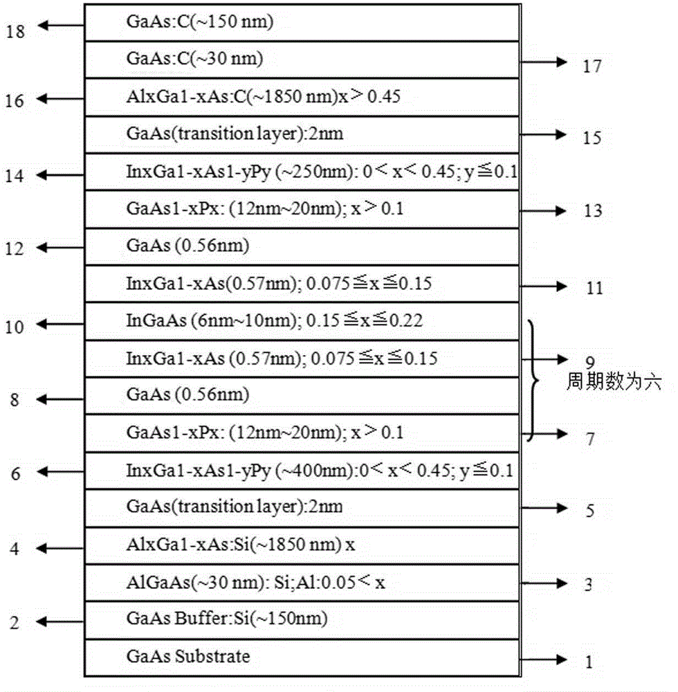
[0042] The present invention will be further described below in conjunction with accompanying drawing:

[0043] Such as figure 1 As shown, a strain-balanced active region gradient potential well layer semiconductor laser structure, including:

[0044] Substrate 1 is an N-type GaAs material of (100) plane;

[0045] The buffer layer 2 is set on the substrate 1 and is made of N-type GaAs material;

[0046] The lower matching layer 3 is set on the buffer layer 2 and is made of N-type AlGaAs material;

[0047] The lower confinement layer 4 is set on the lower matching layer 3 and is made of N-type AlGaAs material;

[0048] The lower transition layer 5 is set on the lower confinement layer 4 and is made of N-type GaAs material;

[0049] The lower waveguide layer 6 is set on the lower transition layer 5 and is made of N-type InGaAsP material;

[0050] Multi-quantum well layer, set on the lower waveguide layer 6, including high In composition InGaAs / low In composition InGaAs / GaAs...


PUM

PropertyMeasurementUnit
Thicknessaaaaaaaaaa
Thicknessaaaaaaaaaa
Thicknessaaaaaaaaaa

Abstract

The invention belongs to the technical field of semiconductor optic electronics and particularly discloses a stain-balance active-area gradient potential well layer semiconductor laser structure. The structure comprises a buffer layer, a lower matching layer, a lower limiting layer, a lower transition layer, a lower waveguide layer, a multiple-quantum well layer, an upper waveguide layer, an upper transition layer, an upper limiting layer, an upper matching layer and an electrode contact layer which are in sequential epitaxial growth from top to bottom by adopting a metal-organic chemical vapor deposition method. Improvements are performed on lowering threshold current of a laser, increasing output power, improving photoelectric conversion efficiency, prolonging service life, improving reliability and the like to obtain the semiconductor laser with the novel structural material system on the basis of improving quality of a material mutation heterogeneous interface of the multiple-quantum well layer, lowering mismatching ratio of strain of lattice constant, reducing mismatching ratio of total accumulated strain of an active area of a quantum well and avoiding lattice relaxation occurring to the quantum well heterogeneous interface.

Description

technical field [0001] The invention relates to the technical field of semiconductor optoelectronics, in particular to a semiconductor laser, in particular to a strain-balanced active region gradient potential well layer semiconductor laser structure. Background technique [0002] High-power semiconductor lasers have a very wide range of applications and market demands in the fields of pumping solid-state lasers and optical fiber lasers, medical fields and communication information fields. As the requirements for laser power become higher and higher, the problem of device reliability becomes more and more prominent. For high-power semiconductor lasers, the optical catastrophe damage on the cavity surface caused by high output optical power density and the temperature rise of the active region and cavity surface caused by various carrier recombination thermal effects become the limit of the maximum output optical power density, affecting A major factor in its reliability and...

Claims


Application Information

Patent Timeline
IPC IPC(8): H01S5/343
Inventor 许并社董海亮马淑芳梁建贾虎生刘旭光
Owner TAIYUAN UNIV OF TECH
Why Eureka
Try Eureka