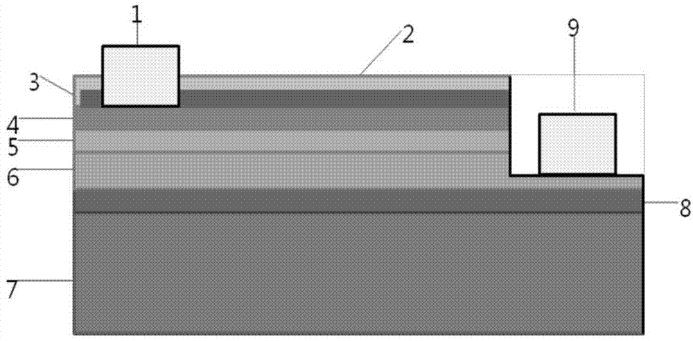
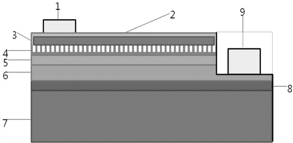
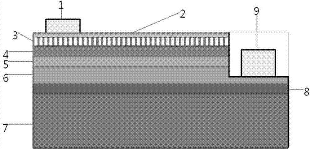
LED chip manufacturing method of high extraction external quantum efficiency
An external quantum efficiency, LED chip technology, applied in electrical components, circuits, semiconductor devices, etc., can solve problems such as high equipment requirements, abnormal chip electrical properties, uncontrolled processes, etc., to improve luminous efficiency, process controlled, An effect that increases the chance of light exiting
- Summary
- Abstract
- Description
- Claims
- Application Information
AI Technical Summary
Problems solved by technology
Method used
Image
Examples
Embodiment 1
[0026] Improving the Quantum Efficiency of LED Chips by Opening P-GaN Microholes
[0027] (1) Epitaxial growth: MOCVD is used to grow the epitaxial layer structure on the sapphire substrate;
[0028] (2) Preparation of P-GaN micropores: The prepared micropore patterns are transferred to the epitaxial P-GaN layer by ICP etching. The micropores are circular holes with a diameter of 1 micron and a period of 3. AZ-510 Photoresist, stepping exposure machine for pattern preparation; the etching power of the upper electrode is 300W, the power of the lower electrode is 60W, and the etching gas and flow rate are respectively: Cl 2 60sccm, BCl 3 20 sccm, Ar 5 sccm, and etching time 45 s, the epitaxial wafer was etched to remove photoresist and clean.
[0029] (3) Pattern preparation: The epitaxy after microhole preparation is prepared for photoresist pattern, and is transferred to the epitaxial structure by ICP etching method. The pattern depth reaches the N-GaN layer, and the etching...
Embodiment 2
[0034] Improving the Quantum Efficiency of LED Chips by Opening ITO Microholes
[0035] (1) Epitaxial growth: MOCVD is used to grow the epitaxial layer structure on the sapphire substrate;
[0036] (2) Pattern preparation: Prepare the photoresist pattern of the epitaxial wafer after epitaxial growth, and transfer it to the epitaxial structure by ICP etching method. The depth of the pattern reaches the N-GaN layer, and the etching depth is about 1.1um. The photolithography pattern is prepared according to the version requirements.
[0037] (3) ITO thin film deposition: After the above-mentioned treatment, epitaxy is cleaned, and an ITO thin film is deposited by E-Gun / sputtering, with a deposition thickness of 60 nm.
[0038] (4) Preparation of ITO micropores: The prepared micropore pattern is transferred to the ITO layer by ICP etching (etching). Glue, stepping exposure machine carries out graphic preparation; Its ICP etching: upper electrode power selects 400W for use, lower...
PUM
| Property | Measurement | Unit |
|---|---|---|
| Etching depth | aaaaa | aaaaa |
| Thickness | aaaaa | aaaaa |
Abstract
Description
Claims
Application Information
 - R&D
- Intellectual Property
- Life Sciences
- Materials
- Tech Scout
- Unparalleled Data Quality
- Higher Quality Content
- 60% Fewer Hallucinations
Browse by: Latest US Patents, China's latest patents, Technical Efficacy Thesaurus, Application Domain, Technology Topic, Popular Technical Reports.
© 2025 PatSnap. All rights reserved.Legal|Privacy policy|Modern Slavery Act Transparency Statement|Sitemap|About US| Contact US: help@patsnap.com


