Device and method for transmission-scattering imaging of nanometer liquid sample in scanning electron microscope

A technology of scanning electron microscopy and liquid samples, which is applied in the direction of material analysis by using radiation and material analysis by measuring secondary emissions. It can solve the problems of increased difficulty, short working distance, and high price, and achieve improved imaging resolution and magnification. The effect of magnification and simple structure

Active Publication Date: 2015-09-09
BEIJING UNIV OF TECH
View PDF5 Cites 24 Cited by
  • Summary
  • Abstract
  • Description
  • Claims
  • Application Information

AI Technical Summary

Problems solved by technology

However, the STEM imaging method has not been popularized in SEM at present, the main reasons are: i) The incident electron energy of SEM (30keV) is much lower than that of TEM incident electron energy (200keV), so that the resolution of STEM image is still significantly lower than that of TEM image , and electron diffraction analysis cannot be carried out in SEM; ii) STEM detectors can only be configured in field emission SEM, which is more expensive; iii) STEM high-resolution imaging requires a short working distance of several mm, and it is difficult to realize in-situ detection of thin film samples Perform CL spectrum and EDS energy spectrum analysis; iv) STEM imaging requires thin film samples, which increases the difficulty of sample preparation

Method used


Image

  • Device and method for transmission-scattering imaging of nanometer liquid sample in scanning electron microscope
  • Device and method for transmission-scattering imaging of nanometer liquid sample in scanning electron microscope
  • Device and method for transmission-scattering imaging of nanometer liquid sample in scanning electron microscope

Examples


Embodiment 1

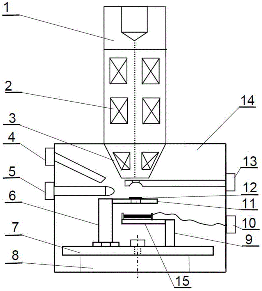
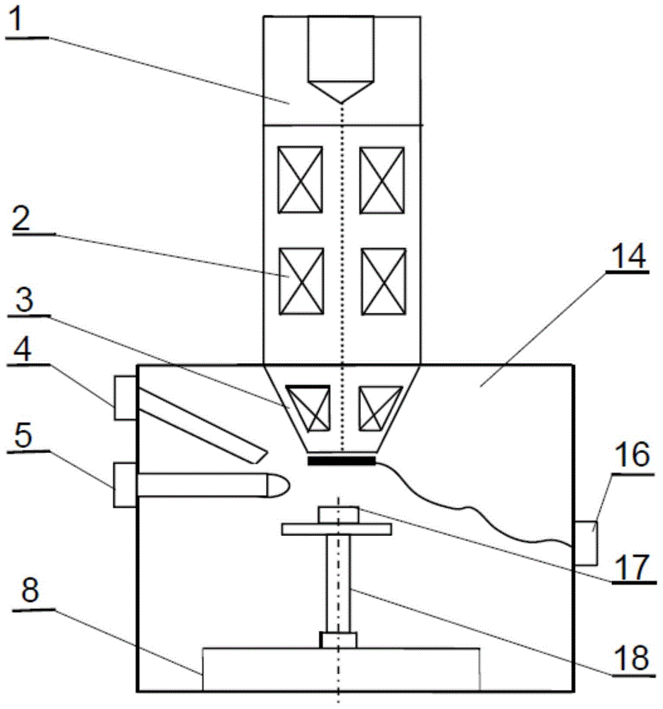
[0053] Embodiment 1: is the scanning electron microscope SEM schematic diagram of the present invention (see figure 1 ), including the sample chamber of the scanning electron microscope SEM and the lens barrel of the scanning electron microscope. In the SEM sample chamber 14 of the scanning electron microscope, a transmission scattered electron detector 10, a nano-liquid sample 12 and corresponding fixing devices are installed. The scanning electron microscope SEM sample room 14 is equipped with a secondary electron detector ETD5, an energy spectrometer EDS4, and a cathode fluorescence spectrometer CL13, which are used in conjunction with the TSD detector 10 to obtain the microscopic morphology, composition, and crystal structure of the nano-liquid sample 12 in situ , band structure and spectral information. As a comparison, figure 2 A schematic diagram of an ordinary scanning electron microscope (SEM) for observing the solid sample 17 is given. There is no TSD detector in...

Embodiment 2

[0054] Embodiment 2: It is the secondary electron SE image of the appearance of the liquid chip, and the magnifications are respectively × 60 and × 250 (see image 3 ). The chip is a square of 2.2 mm×2.2 mm, and the thickness of the upper and lower chips is 200 μm each. A rectangular Si of 400μm×50μm is etched in the middle of the upper and lower chips 3 N 4 Thin window, forming a liquid sink. The thickness of the thin window is 20nm-50nm, and the thickness of the liquid between the upper and lower grooves is 50nm-100nm. The total thickness of the thin window (upper and lower chip plus liquid) reaches 200nm. The liquid drops into the lower chip, with the help of the positioning groove on the right side of the chip ( image 3 (a) Align the upper and lower chips, and seal the chip with epoxy glue.

Embodiment 3

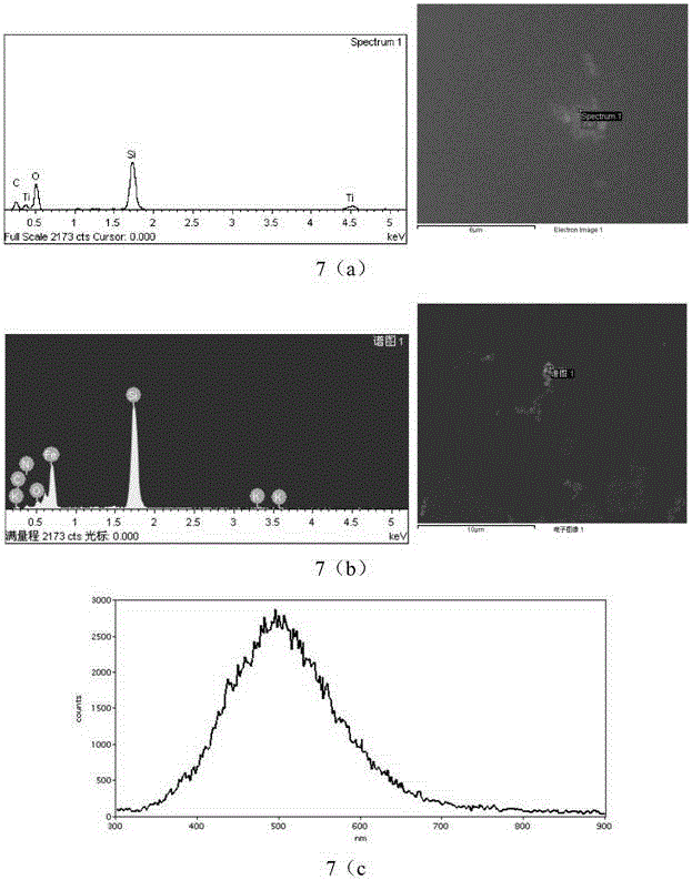
[0055] Embodiment 3: adopt TSD detector and ETD detector, to TiO 2 Liquid chip sample imaging, the acceleration voltage is 30kV, the magnification is ×60000( Figure 4 ).

[0056] Nano-TiO 2 With high activity, good stability, harmlessness, and low recombination rate of photogenerated electrons and holes, it is a photocatalytic material that has attracted much attention and has been widely used in environmental protection, air purification, medical antibacterial and other fields. Under light, TiO 2 The photogenerated holes and OH free radicals generated by the particles have strong oxidizing ability, which can oxidize and decompose organic matter. Nano-TiO 2 Enhanced O 2 The adsorption capacity improves the photocatalytic activity of the liquid phase. In addition, nano-TiO 2 The catalytic activity is closely related to factors such as crystal structure and defects, particle size, light radiation intensity, solvent type and concentration. Therefore, the direct observati...


PUM

PropertyMeasurementUnit
diameteraaaaaaaaaa
diameteraaaaaaaaaa

Abstract

The invention discloses a device and a method for transmission-scattering imaging of a nanometer liquid sample in a scanning electron microscope, belongs to the technical field of electronic micro-analysis devices, and particularly relates to the technical field of reflection and transmission-scattering imaging of the nanometer liquid sample in the scanning electron microscope (SEM). The device and the method are characterized in that a transmission-scattering electronic detector (TSD) is mounted in a sample chamber of the SEM and 5-10 mm under a thin window of the nanometer liquid sample; under the condition that the incident electron energy is 15-30 keV, a transmission-scattering electron image with a resolution ratio of several nanometers, an amplification factor of 50-100000 times and high image contrast can be formed for several to 500 nanometers of nano-particles in a sealed liquid; the TSD is suitable for being mounted in various SEMs, and can be cooperatively used with a secondary electron detector (ETD), an energy disperse spectroscopy (EDS) and a cathode fluorescence spectrometer (CL) for observation of such nanometer-like materials as metal, semiconductors, inorganic matters, organic matters, composites and biological matters.

Description

technical field [0001] The present invention adopts a transmission and scattering electron detector TSD device to observe the nano-liquid sample in the scanning electron microscope SEM, and obtain a transmission and scattering electron image with high resolution (several nm) and high magnification (×100000), combined with an energy spectrometer EDS And cathodofluorescence spectrometer CL, in situ to obtain information on the morphology, composition, crystal structure, energy band structure and emission spectrum of nano liquid chip samples. The nanometer liquid sample is several nanometers to hundreds of nanometer particles sealed in the liquid chip. The TSD detector device has a simple structure and is suitable for use in tungsten filament scanning electron microscopes, field emission scanning electron microscopes, and environmental scanning electron microscopes. The transmission scattering imaging method can be applied in nanotechnology, energy environment, IT industry, biom...

Claims


Application Information

Patent Timeline
Patent Type & Authority Applications(China)
IPC IPC(8): G01N23/04G01N23/22
Inventor 王丽吉元韩晓东皮义群白章鹏严铮洸毛圣成
Owner BEIJING UNIV OF TECH
Why Eureka
Try Eureka