Spectrum detector based on high electron mobility transistor and preparation method thereof

A high electron mobility, spectral detector technology, applied in semiconductor devices, circuits, electrical components, etc., can solve the problems of lack of lattice matching substrates, high cost and volume, film defects, etc., to achieve cost and volume reduction , high sensitivity detection, the effect of improved sensitivity

Active Publication Date: 2015-09-09
BEIJING UNIV OF TECH
View PDF11 Cites 2 Cited by
  • Summary
  • Abstract
  • Description
  • Claims
  • Application Information

AI Technical Summary

Problems solved by technology

[0003] At present, the research on spectral detectors has made some progress, but still faces many difficulties, such as the lack of lattice-matched substrates, the existence of a large number of defects in thin films, etc.
Traditional spectral detectors have poor sensitivity and are costly and bulky enough

Method used


Image

  • Spectrum detector based on high electron mobility transistor and preparation method thereof
  • Spectrum detector based on high electron mobility transistor and preparation method thereof

Examples


preparation example Construction

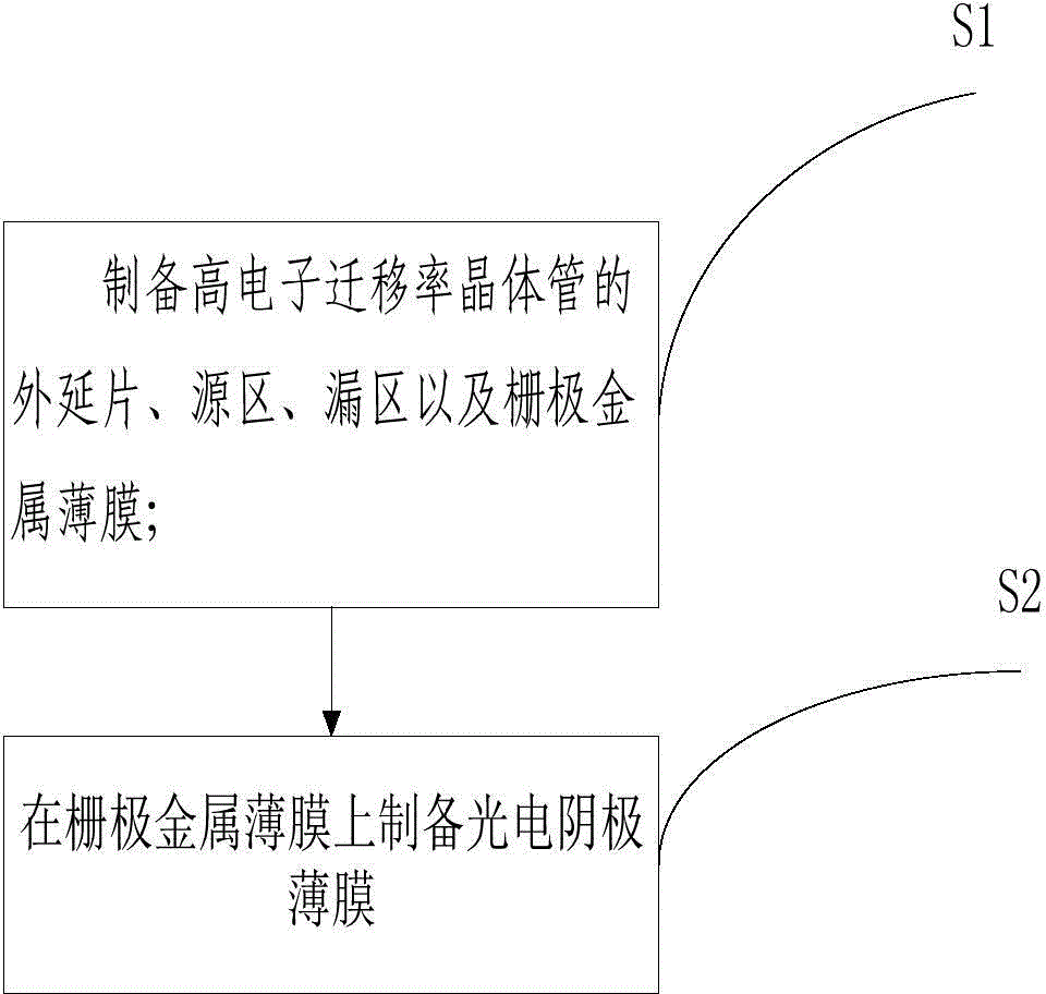
[0037] Corresponding to the above spectral detector, the present invention also discloses a preparation method of a spectral detector based on a high electron mobility transistor, such as figure 2 As shown, the method includes the following steps:

[0038] S1. Prepare epitaxial wafers, source regions, drain regions and gate metal films of high electron mobility transistors;

[0039] S2. Prepare a photocathode thin film on the gate metal thin film.

[0040] Step S1 specifically includes the following steps:

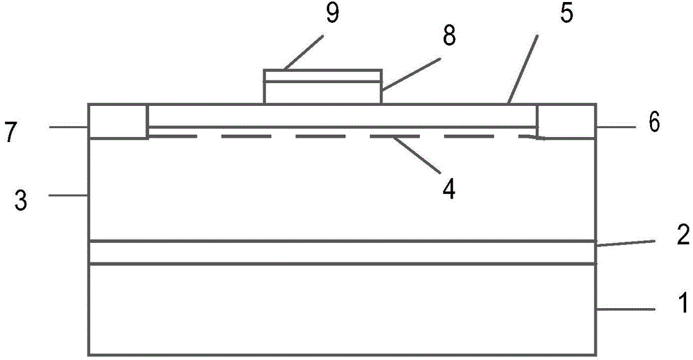
[0041] S11. Prepare an epitaxial wafer including a first semiconductor layer and a second semiconductor layer, wherein the second semiconductor layer covers the upper surface of the first semiconductor layer;

[0042] S12. Prepare a source region and a drain region on both sides of the first semiconductor layer, the source region and the drain region both penetrate the second semiconductor layer, and both the source region and the drain region extend into the first semi...

Embodiment

[0045] Taking GaN / AlGaN HEMT (High Electron Mobility Transistor) as an example, the gate of the HEMT device is a Schottky gate, and the cesium iodide photocathode thin film is used as the light absorption layer. The detection of the visible light spectrum can be realized. In order to make the gate metal and the photocathode material have better adhesion, a layer of titanium Ti metal is sputtered between the gate metal film and the photocathode film, the specific steps are as follows:

[0046]1. First, an epitaxial wafer (first semiconductor layer and second semiconductor layer) with a GaN / AlGaN structure is prepared by a conventional metal organic chemical vapor deposition (MOCVD) process;

[0047] 2. Use the magnetron sputtering system to prepare source-drain electrodes with ohmic contacts;

[0048] 3. Using magnetron sputtering system to prepare gate metal film;

[0049] 4. Prepare Ti metal layer by using magnetron sputtering system;

[0050] 5. Evaporate a layer of cesiu...


PUM


Abstract

The invention relates to a spectrum detector based on a high electron mobility transistor and the preparation method thereof. A photoelectric cathode film layer is arranged on a grid metallic film of the high electron mobility transistor. During spectrum detection, light radiates on the photoelectric cathode film, so that external photoeffect occurs on the photoelectric cathode film. The charge distribution on the surface of the photoelectric cathode film changes, the grid voltage changes, so that the two-dimensional electron gas generated or density in the high electron mobility transistor change. The channel current in the high electron mobility transistor changes accordingly, and the light wave signals are converted into electric signals to detect optical radiation in a highly sensitive means.

Description

technical field [0001] The invention relates to the field of semiconductor optoelectronic information technology, in particular to a spectral detector based on a high electron mobility transistor and a preparation method thereof. Background technique [0002] Detection devices are widely used in guidance, reconnaissance, early warning, detection, tracking, all-weather surveillance and night vision, weapon aiming, electric power online detection, railway vehicle axle temperature detection, mineral resource exploration, underground mine temperature and gas measurement, weather forecast and landform, Military and civilian fields such as environmental monitoring have important military and economic significance. [0003] At present, the research on spectral detectors has made staged progress, but still faces many difficulties, such as the lack of lattice-matched substrates, and the existence of a large number of defects in thin films. Conventional spectral detectors have poor s...

Claims


Application Information

Patent Timeline
Patent Type & Authority Applications(China)
IPC IPC(8): H01L31/10H01L31/18
CPCH01L31/10H01L31/1804Y02P70/50
Inventor 朱彦旭刘飞飞杜志娟郭伟玲于宁邓叶王岳华宋会会
Owner BEIJING UNIV OF TECH
Why Eureka
Try Eureka