A Current Enhanced Lateral Insulated Gate Bipolar Transistor

A bipolar transistor and current enhancement technology, applied in circuits, electrical components, semiconductor devices, etc., can solve problems such as drop in withstand voltage, drop in latch-up suppression capability, increase in device turn-off time, etc., to improve the on-current capability , Improve the latch-up suppression ability, improve the effect of on-current density

Active Publication Date: 2017-10-31
SOUTHEAST UNIV +1
View PDF5 Cites 0 Cited by
  • Summary
  • Abstract
  • Description
  • Claims
  • Application Information

AI Technical Summary

Problems solved by technology

However, while these devices increase the on-current density, they will bring some new problems. For multi-channel LIGBTs, the number of carriers stored in the drift region before turning off is large, and there is no special hole-carrying The sub-draining channel increases the turn-off time of the device, and other technologies to increase the on-current density will also cause problems such as a drop in the withstand voltage of the device or a drop in the ability to resist latch-up.
The drop of the withstand voltage reduces the maximum working voltage of the device, which limits the application of the device; the increase of the off-time increases the switching loss of the device; the latch-up effect will cause the gate signal to lose control of the device, and the device structure may experience Destructive failure, the decline of latch-up suppression ability, which reduces the reliability of the device

Method used


Image

  • A Current Enhanced Lateral Insulated Gate Bipolar Transistor
  • A Current Enhanced Lateral Insulated Gate Bipolar Transistor
  • A Current Enhanced Lateral Insulated Gate Bipolar Transistor

Examples


Embodiment Construction

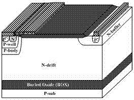
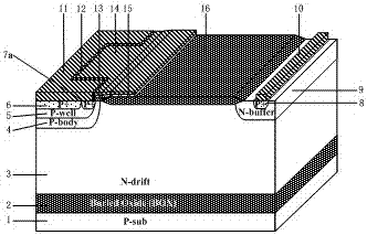
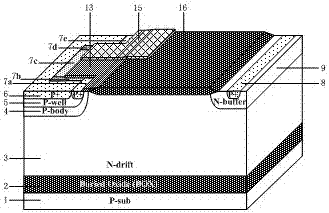
[0030] Combine below figure 2 , image 3 , to describe the present invention in detail, a current-enhanced lateral insulated gate bipolar transistor, comprising: a P-type substrate 1, a buried oxygen 2 is arranged on the P-type substrate 1, and an N-type substrate is arranged on the buried oxygen 2 The drift region 3 is provided with a P-type body region 4 and an N-type buffer region 9 on both sides of the N-type drift region 3, and a heavily doped P-type collector region 8 is arranged in the N-type buffer region 9. Anode metal 10 is connected to the miscellaneous P-type collector region 8, and a field oxide layer 16 is arranged above the N-type drift region 3. One side of the boundary of the field oxide layer 16 is above the N-type buffer zone 9, and the other side is above the N-type buffer zone 9. One side boundary is in contact with the P-type body region 4 and is a straight boundary, a P-type well region 5 is arranged in the P-type body region 4, and a heavily doped P-t...


PUM


Abstract

A current enhanced type lateral insulated gate bipolar transistor improves current density and the turn-off speed on the premise that a latching ability is maintained to be unchanged. The semiconductor is provided with buried oxide disposed on a P-type substrate and an N-drift region disposed on the buried oxide, a P-body region and an N-buffer region are disposed on the N-drift region, a P-type collecting electrode region is disposed in the N-buffer region, an anode metal is connected to the P-type collecting electrode region, a field oxide layer is disposed on the N-drift region, a P-well region is disposed in the P-body region, a P-type emitting electrode region and an emitting electrode region are disposed in the P-well region, the inner-side boundaries of the four regions, i.e., the P-body region, the P-well region, the P-type emitting electrode region and the emitting electrode region are synchronously recessed inwardly to form a square groove, the emitting electrode region surrounding the groove is successively defined as a first P-type emitting electrode region, second, third and fourth N-type emitting electrode regions and a fifth P-type emitting electrode region, the N-drift region protrudes outwardly and fills the square groove, a surface of the P-body region is provided with a gate oxide layer, a surface of the gate oxide layer is provided with a polysilicon layer, and a gate metal is connected to the polysilicon layer.

Description

technical field [0001] The invention mainly relates to the technical field of power semiconductor devices, and is a current-enhanced lateral insulated gate bipolar transistor, which is especially suitable for a high-voltage three-phase single-chip inverter integrated circuit to drive a DC brushless motor. Background technique [0002] Insulated gate bipolar transistor IGBT is a composite power device evolved from the combination of MOS gate device structure and bipolar transistor structure. It has the characteristics of MOS transistor and bipolar transistor, and has good on-state current and switching loss. compromise between them. Silicon-on-Insulator Lateral Insulated Gate Bipolar Transistor (SOI-Lateral Insulated Gate Bipolar Transistor, SOI-LIGBT) is a typical device based on SOI process, with easy integration, high withstand voltage, strong driving current capability, fast switching speed, etc. Advantages, it has been widely used in power integrated circuits. [0003]...

Claims


Application Information

Patent Timeline
Patent Type & Authority Patents(China)
IPC IPC(8): H01L29/739H01L29/06H01L29/08
CPCH01L29/0607H01L29/0808H01L29/7393
Inventor 孙伟锋祝靖张龙顾炎宋华张森苏巍
Owner SOUTHEAST UNIV
Why Eureka
Try Eureka