A Low Noise and Low Loss Insulated Gate Bipolar Transistor
A bipolar transistor, low-loss technology, used in semiconductor devices, semiconductor/solid-state device manufacturing, electrical components, etc., to reduce noise and speed up turn-on
- Summary
- Abstract
- Description
- Claims
- Application Information
AI Technical Summary
Problems solved by technology
Method used
Image
Examples
Embodiment 1
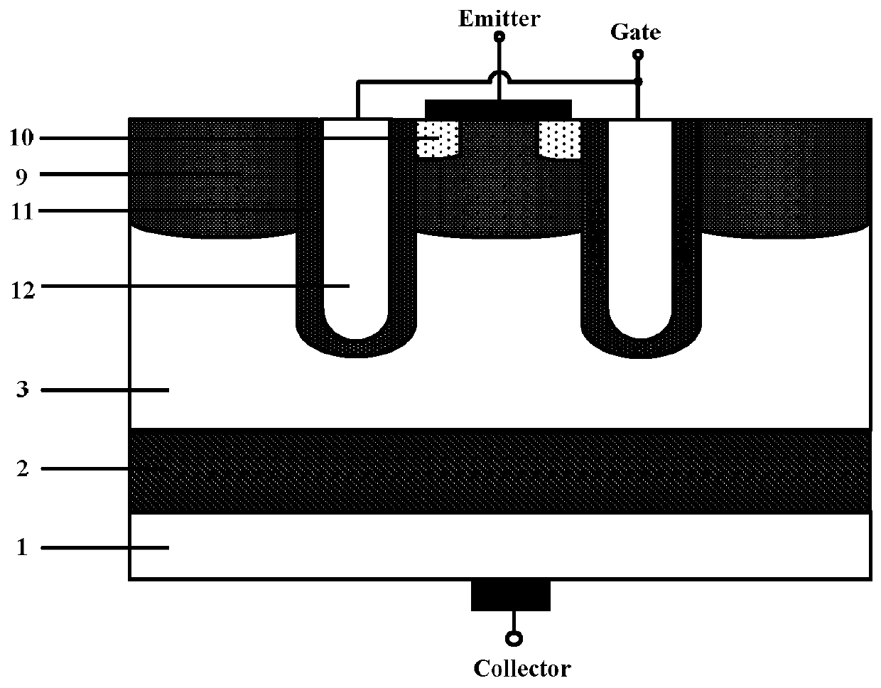
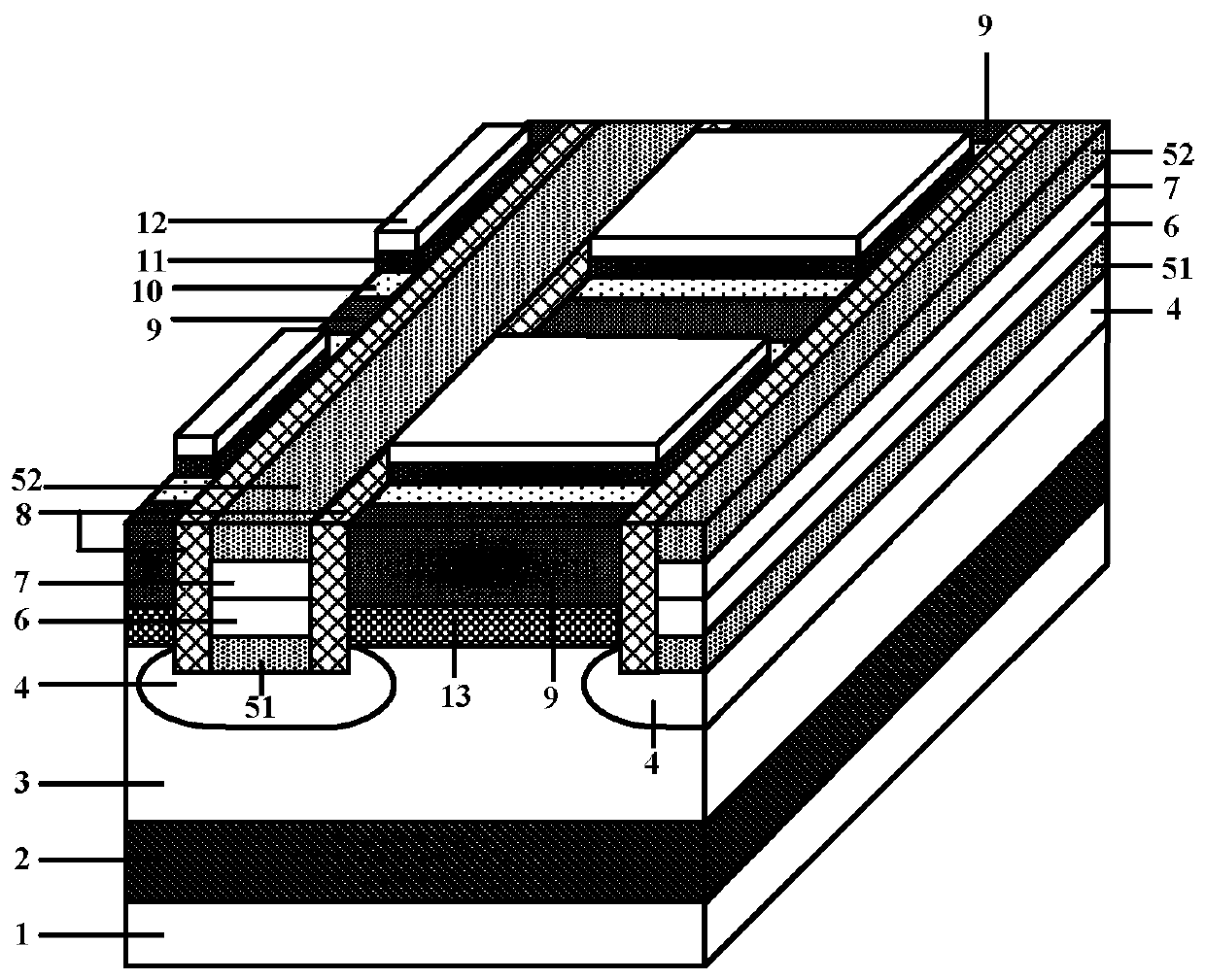
[0030] Combine below Figure 3-4 , to describe the present invention in detail, a low-noise and low-loss insulated gate bipolar transistor, comprising: a P-type substrate 1, an anode metal layer is arranged at the bottom of the P-type substrate 1 and serves as the collector of the device, An N-type buffer layer 2 is arranged above the P-type substrate 1, an N-type epitaxial layer 3 is arranged on the N-type buffer layer 2, and a P-type body region 9 distributed in a one-dimensional array is arranged in the N-type epitaxial layer 3, On both sides of the part of the N-type epitaxial layer between adjacent P-type body regions 9, heavily doped N-type emitter regions 10 are respectively provided, and the heavily doped N-type emitter regions are located in the corresponding P-type body regions 9, It is characterized in that the transistor also includes trenches whose sidewalls are distributed in a one-dimensional array and covered with an isolation oxide layer 8, and each trench tra...
Embodiment 2
[0032] A method for preparing a low-noise and low-loss insulated gate bipolar transistor, comprising:
[0033] The first step: first select N-type silicon material as the substrate and epitaxially grow shallowly doped N-type epitaxial layer;
[0034] The second step: ion implantation of N-type impurities, and annealing to form a lightly doped N-type carrier storage layer 13;
[0035] Step 3: etching the trench and forming an isolation oxide layer 8;
[0036] The fourth step: ion implantation of P-type impurities, and annealing to form P-type body region 9;
[0037] Step 5: The ion implantation dose range at the bottom of the trench is 1e13cm -2 to 1e18cm -2 , P-type impurities with an energy of 80Kev, and annealed to form a heavily doped P well 4;
[0038] Step 6: Deposit metal in the trench to form a metal connection layer-51;
[0039] Step 7: Deposit polysilicon in the trench, and the ion implantation dose is greater than 1e17cm -2 The P-type impurities form the diode ...
Embodiment 3
[0049] A low-noise and low-loss insulated gate bipolar transistor, comprising: a P-type substrate 1, an anode metal layer is provided at the bottom of the P-type substrate 1 and serves as a collector of the device, above the P-type substrate 1 An N-type buffer layer 2 is provided, an N-type epitaxial layer 3 is arranged on the N-type buffer layer 2, and a P-type body region 9 distributed in a one-dimensional array is arranged in the N-type epitaxial layer 3. Both sides of the part of the N-type epitaxial layer between the regions 9 are respectively provided with heavily doped N-type emitter regions 10, and the heavily doped N-type emitter regions are located in the corresponding P-type body regions 9, refer to Figure 15 , the transistor also includes trenches whose sidewalls are distributed in a one-dimensional array and covered with an isolation oxide layer 8, and each trench traverses through each P-type body region 9, heavily doped N-type emitter region 10 and N-type epitax...
PUM
 Abstract
Description
Claims
Application Information


