

A composite gate igbt chip with three-dimensional channel
A compound gate and chip technology, applied in semiconductor devices, electrical components, circuits, etc., to achieve the effect of reducing on-voltage drop, small parasitic capacitance, and reducing parasitic resistance
- Summary
- Abstract
- Description
- Claims
- Application Information
AI Technical Summary
Problems solved by technology
Method used
Image

Examples
no. 1 example
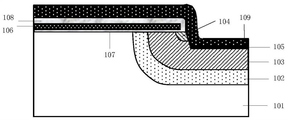
[0041] The composite gate IGBT chip of this embodiment includes a plurality of cells. In order to more clearly illustrate the composite gate IGBT chip of this embodiment, the following uses Figure 4 The schematic diagram of the structure of a single bar-shaped cell is shown as an example for detailed explanation.
[0042] Figure 4 It is a schematic structural diagram of a composite gate IGBT chip with a three-dimensional channel in the first embodiment of the present invention. Such as Figure 4As shown, it includes a substrate 1 , cells disposed on the substrate 1 , and an N-type buffer layer 2 , a P-type layer 3 and an anode metal layer 4 disposed below the substrate 1 . Among them, the cell mainly includes: a trench polysilicon gate electrode 5, a first oxide layer 6, two P well regions 7, two doped regions (the doped regions include N++ doped regions 8 and P++ doped regions 9), Two second oxide layers 10 , two planar polysilicon gate electrodes 11 , two third oxide l...
no. 2 example
[0058] This embodiment is a further optimization of the first embodiment.
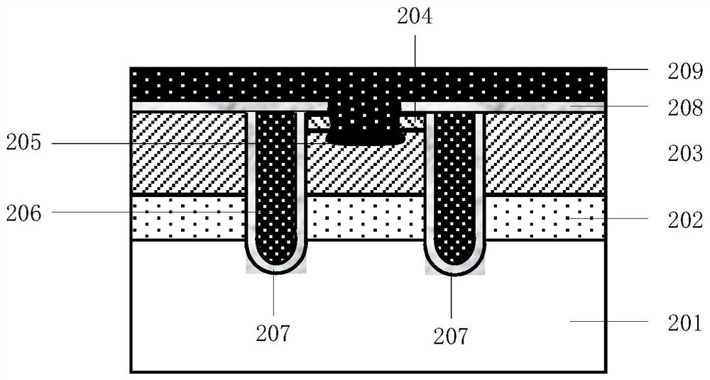
[0059] Figure 5 It is a schematic structural diagram of a composite gate IGBT chip with a three-dimensional channel in the second embodiment of the present invention. Such as Figure 5 shown in Figure 4 An N well region 15 is added to the shown cell. The N well region 15 is located below the P well region 7 and is in contact with the lower surface and the side of the P well region 7 , and the width of the N well region 15 is greater than that of the P well region 7 .
[0060] In this embodiment, an N well region is added around the P well region to further increase the conductance modulation effect of the IGBT chip in the drift region.
PUM
 Abstract
Description
Claims
Application Information