Organic electroluminescent light emitting device and preparation method thereof

An electroluminescent device and electroluminescent technology, which are applied in the fields of electro-solid devices, semiconductor/solid-state device manufacturing, electrical components, etc., can solve the problems of reducing luminous efficiency, adverse effects on device life, etc., so as to improve luminous efficiency and improve luminous efficiency. , the effect of strong reflection

Inactive Publication Date: 2015-09-23
OCEANS KING LIGHTING SCI&TECH CO LTD +2
View PDF0 Cites 10 Cited by
  • Summary
  • Abstract
  • Description
  • Claims
  • Application Information

AI Technical Summary

Problems solved by technology

[0003] In a typical organic electroluminescent device, the injection efficiency and transport ability of holes are generally higher than that of electrons, and a considerable part of the holes constitute leakage current, which reduces the luminous efficiency and adversely affects the life of the device.

Method used


Image

  • Organic electroluminescent light emitting device and preparation method thereof
  • Organic electroluminescent light emitting device and preparation method thereof

Examples


Embodiment 1

[0054] A method for preparing an organic electroluminescent device, comprising the following steps:

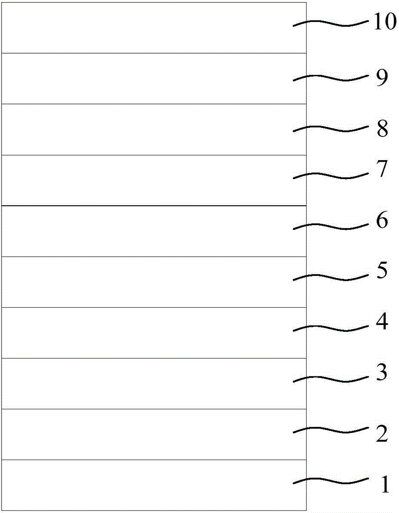
[0055] (1) Rinse the commercially available common glass substrate with distilled water and ethanol, and soak it in isopropanol for one night. The anode 2 is prepared on the glass substrate 1 by magnetron sputtering. The material of the anode 2 is ITO, the thickness is 110nm, the acceleration voltage of the magnetron sputtering is 700V, the magnetic field is about 120G, and the power density is 25W / cm 2 ; Then on the anode 2, the thermal resistance evaporation hole injection layer 3 and the hole transport layer 4 are sequentially deposited; wherein the material of the hole injection layer is MoO 3 , the thickness is 33nm, and the pressure used in evaporation is 8×10 -4 Pa, the evaporation rate is 2nm / s; the material of the hole transport layer is NPB, the thickness is 50nm, and the pressure used in the evaporation is 8×10 -4 Pa, the evaporation rate is 0.2nm / s;

[0056] (2)...

Embodiment 2

[0063] A method for preparing an organic electroluminescent device, comprising the following steps:

[0064] (1) Rinse the commercially available common glass substrate with distilled water and ethanol, and soak it in isopropanol for one night. The anode is prepared on the glass substrate by magnetron sputtering. The material of the anode is AZO, the thickness is 300nm, the acceleration voltage of magnetron sputtering is 300V, the magnetic field is about 50G, and the power density is 40W / cm 2 ; Then on the anode, the thermal resistance evaporation hole injection layer and the hole transport layer are sequentially deposited; wherein the material of the hole injection layer is V 2 o 5 , the thickness is 20nm, and the pressure used in evaporation is 2×10 -3 Pa, the evaporation rate is 10nm / s; the material of the hole transport layer is TCTA, the thickness is 50nm, and the pressure used in the evaporation is 2×10 -3 Pa, the evaporation rate is 1nm / s;

[0065] (2) On the hole t...

Embodiment 3

[0072] A method for preparing an organic electroluminescent device, comprising the following steps:

[0073] (1) Rinse the commercially available common glass substrate with distilled water and ethanol, and soak it in isopropanol for one night. The anode is prepared on the glass substrate by magnetron sputtering. The material of the anode is IZO, the thickness is 150nm, the acceleration voltage of magnetron sputtering is 800V, the magnetic field is about 200G, and the power density is 1W / cm 2 ; Then on the anode, the thermal resistance evaporation hole injection layer and the hole transport layer are sequentially deposited; wherein the material of the hole injection layer is V 2 o 5 , the thickness is 55nm, and the pressure used in evaporation is 5×10 -5 Pa, the evaporation rate is 1nm / s; the material of the hole transport layer is TAPC, the thickness is 60nm, and the pressure used in the evaporation is 5×10 -5 Pa, the evaporation rate is 0.1nm / s;

[0074] (2) On the hole ...


PUM


Abstract

The present invention discloses an organic electroluminescent light emitting device which comprises a glass substrate, an anode, a hole injection layer, a hole transmission layer, an electron blocking layer, a light emitting layer, a hole blocking layer, an electron transmission layer, an electron injection layer and a cathode which are stacked in order. The material of the electron blocking layer is the mixed material of a bipolar organic material and a zinc compound. The material of the hole blocking layer is the mixed material of a metal sulfide and a phosphorescent material. A hole can be blocked by the hole blocking layer of the organic electroluminescent light emitting device well, the recombination of the hole in the electron transmission layer can be avoided, the reflection of light is improved, and the light emitting efficiency is improved. Electrons can be effectively prevented from going into the hole transmission layer to recombine by the electron block layer, the transmission of the hole is facilitated, and finally the light emitting efficiency of the organic electroluminescent light emitting device is improved.

Description

technical field [0001] The invention relates to the field of organic electroluminescence, in particular to an organic electroluminescence device and a preparation method thereof. Background technique [0002] Organic light-emitting devices (Organic light-emitting devices, referred to as OLEDs) is a multi-layer light-emitting device using organic light-emitting materials, including sequentially stacked anode layer, hole injection layer, hole transport layer, light-emitting layer, electron transport layer layer and cathode. The luminescent principle of OLED is based on the action of an external electric field, electrons are injected from the cathode to the lowest unoccupied molecular orbital (LUMO) of organic matter, and holes are injected from the anode to the highest occupied orbital (HOMO) of organic matter. The light-emitting layers meet, recombine, and form excitons. The excitons migrate under the action of the electric field and transfer energy to the light-emitting mat...

Claims


Application Information

Patent Timeline
Patent Type & Authority Applications(China)
IPC IPC(8): H01L51/50H01L51/54H01L51/56
CPCH10K85/00H10K50/17H10K50/171H10K71/00
Inventor 周明杰黄辉张振华王平
Owner OCEANS KING LIGHTING SCI&TECH CO LTD
Why Eureka
Try Eureka