Optical module

A technology of optical modules and optical paths, applied in the field of optical modules, can solve problems such as signal transmission loss, solve heat dissipation problems, and achieve heat dissipation effects

Active Publication Date: 2015-10-07
HISENSE BROADBAND MULTIMEDIA TECH
View PDF5 Cites 20 Cited by
  • Summary
  • Abstract
  • Description
  • Claims
  • Application Information

AI Technical Summary

Problems solved by technology

[0005] For high-speed, high-power driver chips, the high-speed signal will be lost in the gold wire, and the flip chip under the driver chip 2 (flip chip: deposit tin-lead balls on the input and output ends of the chip, due to the input and output The distribution of the leads and the entire surface of the chip, then all the tin-lead balls are distributed on the entire lower surface of the chip) to connect the pins of the driver chip with the lines on the printed circuit board to achieve communication. In this case, although it is solved The problem of signal transmission loss, but because the driver chip 2 covered by the lens assembly is a tin-lead ball for signal transmission, it is no longer possible to use the method of laying copper under the driver chip to dissipate the heat generated by the driver chip

Method used


Image

  • Optical module
  • Optical module
  • Optical module

Examples


Embodiment Construction

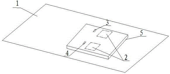
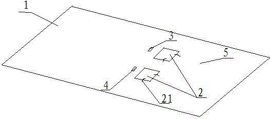
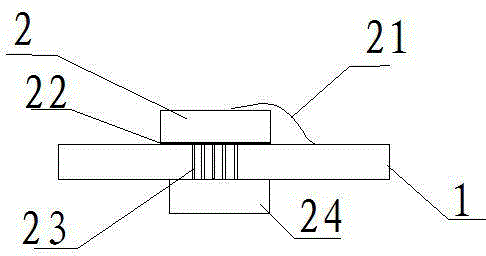
[0018] The embodiment of the present application provides an optical module to solve the heat dissipation problem of the driver chip in the optical module; a heat sink is mounted on the surface of the driver chip buckled by the lens assembly cover, and the heat sink is connected with the heat sink laid on the circuit board. The heat conduction layer is connected, and the heat conduction layer is partly or completely laid outside the space of the lens assembly cover buckle, and conducts the heat emitted by the driver chip out of the lens component cover buckle space, realizing the technical effect of dissipating heat.

[0019] In order to better understand the above technical solution, the above technical solution will be described in detail below in conjunction with the accompanying drawings and specific implementation manners.

[0020] Such as Figure 4 with Figure 7 As shown, it is a schematic structural diagram of the optical module proposed in the embodiment of the prese...


PUM


Abstract

The invention provides an optical module, and solves a problem of heat radiation of a drive chip covered by a lens assembly. The optical module comprises a circuit board, the lens assembly, a laser device or a detector, the drive chip, a heat-radiating fin which is surface-mounted on the upper surface of the drive chip, and a heat-conducting layer which is laid on the circuit board. The laser device, the detector and the drive chip are surface-mounted on the circuit board and are covered by the lens assembly. The heat-radiating fin is downwardly bent from the upper surface of the drive chip and then connected with the heat-conducting layer. Partial or the entire heat-conducting layer is laid on the part of the circuit board without coverage of the lens assembly. The heat-radiating fin is surface-mounted on the upper surface of the drive chip in the coverage space of the lens assembly, and the heat-radiating fin and the heat-conducting layer are connected to form a heat radiation path so that heat radiated by the drive chip in the coverage space of the lens assembly is conducted out of the space and thus the technical effect of heat radiation is realized.

Description

technical field [0001] The invention relates to the technical field of optical fiber communication, in particular to an optical module. Background technique [0002] In the field of optical fiber communication technology, the optical module converts the electrical signal into an optical signal before sending it, and converts the received optical signal into an electrical signal, which plays the role of photoelectric conversion. Typically includes circuit boards, chips, photodetectors, lasers, lens assemblies and heat sinks. [0003] Such as figure 1 As shown, in the optical communication COB (Chip On Broad, that is, the bare chip is glued on the interconnection substrate with conductive or non-conductive adhesive, and then wire bonded to achieve electrical connection) packaging technology, the driver chip 2 is directly mounted On the printed circuit board 1 , it is used to drive the laser 3 or the detector 4 ; a lens assembly 5 is placed above the driving chip 2 . For rel...

Claims


Application Information

Patent Timeline
Patent Type & Authority Applications(China)
IPC IPC(8): G02B6/42
CPCG02B6/4269G02B6/428G02B6/4296
Inventor 司宝峰刘旭霞黄永亮
Owner HISENSE BROADBAND MULTIMEDIA TECH
Why Eureka
Try Eureka