Method for reducing dark current of image sensor

An image sensor and device technology, applied in the field of semiconductors, can solve the problems of increased thermal electron injection effect and interface state increase in transfer tubes, and achieve the effects of suppressing the generation probability, reducing the electric field, and increasing the effective channel length

Active Publication Date: 2015-10-21
SHANGHAI HUALI MICROELECTRONICS CORP
View PDF4 Cites 3 Cited by
  • Summary
  • Abstract
  • Description
  • Claims
  • Application Information

AI Technical Summary

Problems solved by technology

However, as the size of the pixel unit shrinks, the size of the photodiode PD and the transfer transistor Tx will also continue to shrink. For the drain end of the transfer transistor Tx (ie, the floating diffusion point FD), the lightly doped drain region (LDD) is placed on the Before the formation of the side wall (spacer), the effective channel length of the transfer tube will be reduced, and the hot electron injection effect of the transfer tube will increase. These hot electrons break the original Si-H bond and increase the interface state.

Method used


Image

  • Method for reducing dark current of image sensor
  • Method for reducing dark current of image sensor
  • Method for reducing dark current of image sensor

Examples


Embodiment Construction

[0019] In order to make the content of the present invention clearer and easier to understand, the content of the present invention will be further described below in conjunction with the accompanying drawings. Of course, the present invention is not limited to this specific embodiment, and general replacements known to those skilled in the art are also covered within the protection scope of the present invention.

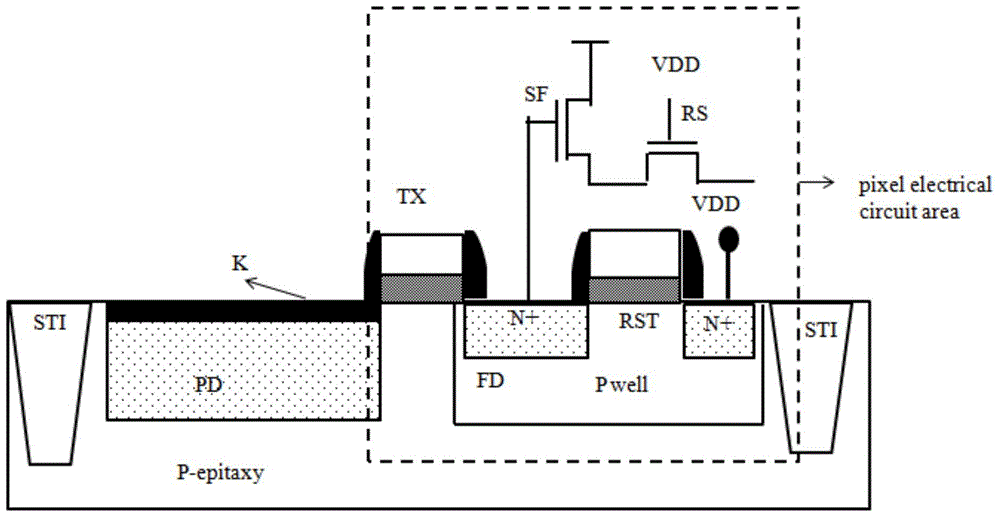
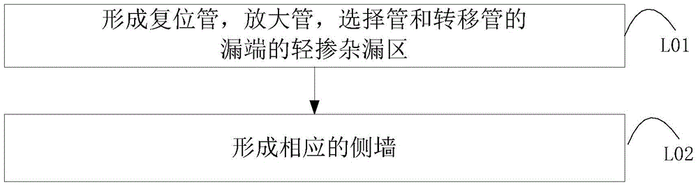
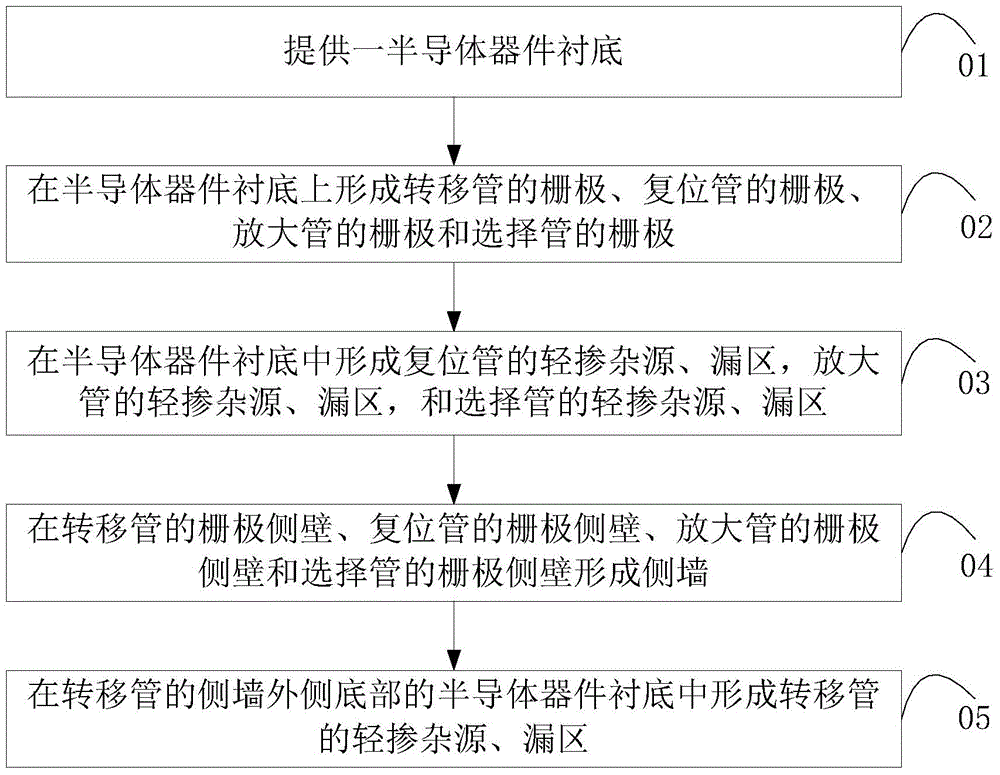
[0020] In the present invention, the image sensor includes a photodiode and a transistor, and the transistor includes a transfer transistor, a reset transistor, an amplifier transistor and a selection transistor, and the lightly doped drain region of the transfer transistor is a floating diffusion point; the method of reducing the dark current of the image sensor of the present invention Methods, including the fabrication of photodiodes and the fabrication of transistors. In the process of transistor preparation, the gates of the above four transistors are first fo...


PUM


Abstract

The invention provides a method for reducing dark current of an image sensor. The method comprises preparation of a photodiode and a transistor. The preparation of the transistor comprises following steps of firstly forming grid electrodes of four transistors; forming light dope drain regions of a reset pipe, an amplifying pipe and a selecting pipe; then, forming corresponding side walls on grid electrode side walls of the rest pipe, the amplifying pipe, the selection pipe and a transferring pipe; and at last, forming a light dope drain region of the transferring pipe on the substrate of a semiconductor at the bottom of the outer side of the side wall of the transferring pipe. Thus, effective channel length of the transferring pipe is increased, electric field in the channel direction is reduced and probability of generation of thermal electrons is reduced, thereby reducing dark current of the image sensor.

Description

technical field [0001] The invention relates to the technical field of semiconductors, in particular to a method for reducing dark current of an image sensor. Background technique [0002] CMOS image sensor (CIS) is compatible with the existing integrated circuit manufacturing process because of its manufacturing process, and has many advantages in performance compared with the original charge-coupled device CCD. The CMOS image sensor can integrate the driving circuit and the pixel together, which simplifies the hardware design and reduces the power consumption of the system at the same time. Because CIS can take out electrical signals while collecting optical signals, it can also process image information in real time, and its speed is faster than that of CCD image sensors. CMOS image sensors also have the advantages of low price, large bandwidth, anti-blur, flexible access and large fill factor. [0003] Traditional active pixels use photodiodes as image sensing devices....

Claims


Application Information

Patent Timeline
Patent Type & Authority Applications(China)
IPC IPC(8): H01L27/146
Inventor 田志陈昊瑜
Owner SHANGHAI HUALI MICROELECTRONICS CORP
Why Eureka
Try Eureka