High-speed CMOS monolithically integrated optical receiver with full bandwidth single-ended-to-differential

A single-ended to differential, monolithic integration technology, applied in the direction of electromagnetic receivers, can solve problems such as difficult to find, achieve the effect of reducing the number of uses, shielding the Miller effect, and improving bandwidth

Inactive Publication Date: 2015-10-21
TIANJIN UNIV
View PDF3 Cites 18 Cited by
  • Summary
  • Abstract
  • Description
  • Claims
  • Application Information

AI Technical Summary

Problems solved by technology

In the design process of transimpedance amplifiers, bandwidth and noise are contradictory, and it is difficult to find a solution that is both excellent

Method used


Image

  • High-speed CMOS monolithically integrated optical receiver with full bandwidth single-ended-to-differential
  • High-speed CMOS monolithically integrated optical receiver with full bandwidth single-ended-to-differential
  • High-speed CMOS monolithically integrated optical receiver with full bandwidth single-ended-to-differential

Examples


Embodiment 1

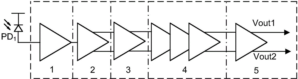
[0041] A high-speed CMOS monolithic integrated optical receiver with full bandwidth single-ended to differential, see figure 1 , this high-speed CMOS monolithic integrated optical receiver includes:

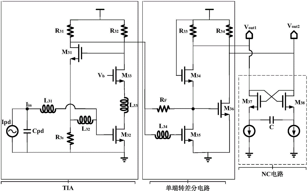
[0042] The high-bandwidth adjustable cascode transimpedance amplifier 1 is used to convert the current signal output by the photodetector into a voltage signal for preliminary amplification;

[0043] A single-ended to differential converter 2 with a negative capacitance circuit is used to realize single-ended to differential conversion, improve bandwidth and amplify voltage signals;

[0044] The DC offset elimination unit 3 is used to eliminate the DC offset of the interleaved active feedback limiting amplifier 4 caused by the unbalanced signal output by the single-ended to differentiator 2, so that the common mode of the interleaved active feedback limiting amplifier 4 The level is consistent;

[0045] The interleaved active feedback limiting amplifier 4 is used to amplify the...

Embodiment 2

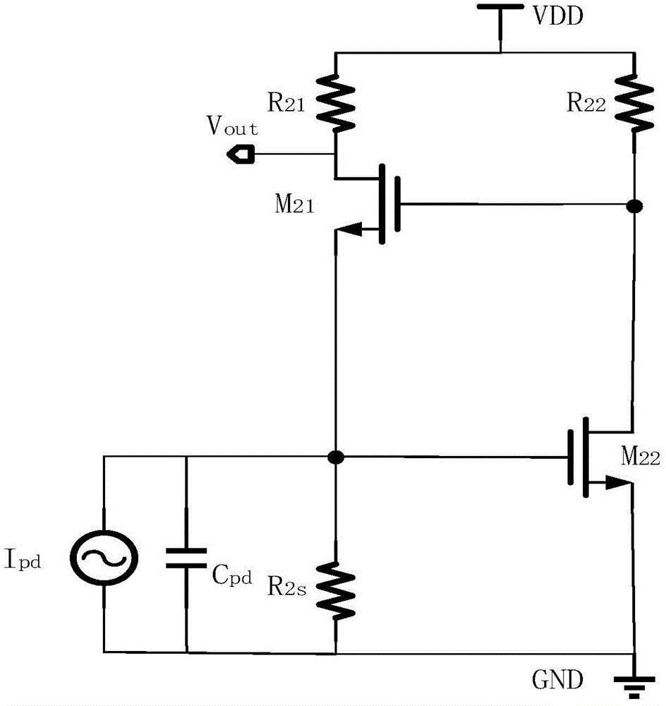
[0056] In order to more clearly describe the structure and working principle of the high-bandwidth RGC transimpedance amplifier 1 proposed by the present invention, and highlight the many advantages of the high-bandwidth RGC transimpedance amplifier 1 designed by the present invention compared with the traditional RGC transimpedance amplifier, the following briefly describes The working principle of the traditional RGC transimpedance amplifier, and then describe the working principle of the high-bandwidth RGC transimpedance amplifier 1 in detail from the aspects of expanding bandwidth and reducing noise.

[0057] The present invention comprehensively utilizes the following four technologies to expand the bandwidth, that is, cascode feedback channel reduces input impedance, Miller capacitance "shielding" effect, Butterworth LC ladder matching network and π-type broadband matching network. Among them, the Butterworth LC ladder matching network can effectively reduce the equivalen...


PUM


Abstract

The invention discloses a high-speed CMOS monolithically integrated optical receiver with full bandwidth single-ended-to-differential, comprising a high bandwidth adjustment type cascode transimpedance amplifier used for converting a current signal output by a photoelectric detector into a voltage signal and preliminarily amplifying the voltage signal; a single-ended-to-differential device provided with a negative capacitance circuit and used for achieving single-ended-to-differential conversion and increasing a bandwidth and an amplified voltage signal; a DC offset eliminating unit used for eliminating a DC offset of an interleaved active feedback limiting amplifier caused by an unbalanced signal output by the single-ended-to-differential device and ensuring a uniform common mode level for the interleaved active feedback limiting amplifier; the interleaved active feedback limiting amplifier, used for amplifying the voltage signal output by the high bandwidth adjustment type cascode transimpedance amplifier to a voltage level required by a digital processing unit; and an output buffer stage used for providing driving ability. While improving the circuit gain, the high-speed CMOS monolithically integrated optical receiver disclosed by the invention is used for expanding the working bandwidth and overcoming the shortcomings in the prior art.

Description

technical field [0001] The invention relates to the field of optical fiber communication system and optical interconnection, in particular to a high-speed CMOS single-chip integrated optical receiver based on an adjustable cascode (RGC) circuit structure and full bandwidth single-end to differential conversion. Background technique [0002] As human society's demand for network bandwidth and data traffic increases exponentially. The ultra-high-speed and ultra-large-capacity optical fiber communication technology for trunk network transmission has made breakthroughs, but electronic information processing is still used for short-distance communication between cabinets, circuit boards, chips, and inside chips of optical network switching nodes. And exchange methods, which limit the further improvement of information processing speed. Therefore, in short distances and very short distances, it has become an inevitable trend to replace electrical interconnections with optical int...

Claims


Application Information

Patent Timeline
Patent Type & Authority Applications(China)
IPC IPC(8): H04B10/60
Inventor 谢生高谦毛陆虹陶希子吴思聪
Owner TIANJIN UNIV
Why Eureka
Try Eureka