Heat sink structure double-carrier LED drive circuit package and manufacturing method thereof

A technology of LED driving and circuit packaging, applied in circuits, electrical components, electric solid devices, etc., can solve the problems of dissipation, mutual penetration of insulating glue and conductive glue, and difficulty in heat of LED driving circuit, etc., to increase the thickness, The effect of enhancing the ability to withstand high pressure leak points

Inactive Publication Date: 2015-11-04
TIANSHUI HUATIAN TECH +1
View PDF4 Cites 4 Cited by
  • Summary
  • Abstract
  • Description
  • Claims
  • Application Information

AI Technical Summary

Problems solved by technology

When applied under high voltage conditions, the large amount of heat emitted by the MOSFET power device in the LED drive circuit is difficult to effectively dissipate through the conduction of the lead frame
At the same time, due to the effect of high temperature and high pressure, the insulating glue at the bottom of the IC chip is easily broken down and leakage occurs; in addition, because the lead frame is a single carrier structure, the insulating glue and conductive glue on the surface of the carrier are easy to penetrate each other, resulting in leakage

Method used


Image

  • Heat sink structure double-carrier LED drive circuit package and manufacturing method thereof
  • Heat sink structure double-carrier LED drive circuit package and manufacturing method thereof
  • Heat sink structure double-carrier LED drive circuit package and manufacturing method thereof

Examples


Embodiment 1

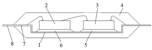
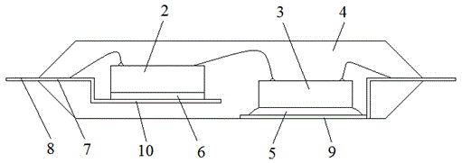
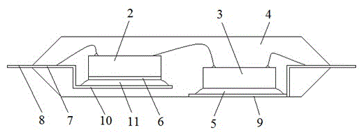
[0027]The insulating adhesive is coated on the back of the wafer by the wafer back coating process to form an insulating adhesive film with a thickness of 100 μm; then the wafer is cut into individual crystal grains to obtain IC control chips; then, the insulating adhesive is applied by dispensing process The slurry is drip-coated on the surface of the second base island. After the insulating slurry is cured, an insulating slurry layer with a thickness of 5 μm is formed, and then the IC control chip coated with an insulating adhesive layer on the back is pasted on the second base island. surface; paste the MOSFET power device on the upper surface of the first base island; use the existing production process of the LED drive circuit with built-in MOSFET devices for pressure welding, plastic packaging, curing and testing; during the plastic packaging process, the first base island is not pasted The bottom surface of the device is located outside the encapsulant, and a heat sink s...

Embodiment 2

[0029] The insulating adhesive is coated on the back of the wafer by the wafer back coating process to form an insulating adhesive film with a thickness of 20 μm; then the wafer is cut into individual crystal grains to obtain an IC control chip, and then the IC control chip is pasted on the second wafer. The upper surface of the second base island; paste the MOSFET power device on the upper surface of the first base island; adopt the existing production process of the LED drive circuit with built-in MOSFET device for pressure welding, plastic sealing, curing and testing; during the plastic sealing process, make the second base island The bottom surface of the base island without the pasted device is located outside the sealant, and a dual-carrier LED drive circuit package with a heat sink structure is prepared.

Embodiment 3

[0031] The insulating adhesive is coated on the back of the wafer by the wafer back coating process to form an insulating adhesive film with a thickness of 60 μm; then the wafer is cut into individual crystal grains to obtain IC control chips; then, the insulating adhesive is applied by dispensing process The slurry is drip-coated on the surface of the second base island. After the insulating slurry is cured, an insulating slurry layer with a thickness of 35 μm is formed, and then the IC control chip coated with an insulating adhesive layer on the back is pasted on the second base island. surface; paste the MOSFET power device on the upper surface of the first base island; use the existing production process of the LED drive circuit with built-in MOSFET devices for pressure welding, plastic packaging, curing and testing; during the plastic packaging process, the first base island is not pasted The bottom surface of the device is located outside the encapsulant, and a heat sink ...


PUM


Abstract

The invention discloses a heat sink structure double-carrier LED (Light-Emitting Diode) drive circuit package and a manufacturing method thereof. The package comprises a power device and a control chip both fixed on base islands, the control chip is connected with the power device and an inner pin, the power device is connected with the inner pin, the inner pin is connected with an external pin, and sealant bodies are arranged on the base islands by plastic packaging; the base islands are two mutually isolated base islands, the power device is adhered on one base island through a conductive adhesive film, and the bottom surface of the base island, opposite to the power device, is located outside the sealant body; and an IC control chip is adhered on the other base island through an insulating adhesive film. The back surface of a wafer is coated with an insulation paste, the wafer is adhered on the base island after being cut into single crystalline grains, the power device is adhered on the other base island, and pressure welding, plastic packaging, curing and detection are carried out through the existing technology; the bottom surface of the first base island, without any adhered device, is located outside the sealant body, and thus, the heat sink structure double-carrier LED drive circuit package is obtained. The package can quickly dissipate a large amount of heat, the insulation paste is not liable to be broken down, and the insulation paste and the conductive adhesive are not interpenetrative to each other.

Description

technical field [0001] The invention belongs to the technical field of semiconductor packaging for electronic device manufacturing, and relates to an LED drive circuit package, in particular to a heat sink structure double-carrier LED drive circuit package; the invention also relates to a manufacturing method of the package. Background technique [0002] A light-emitting diode (Light-Emitting Diode, referred to as LED) is a semiconductor electronic component that can convert electrical energy into light energy. It is called the fourth-generation light source. High brightness, waterproof, miniature, shockproof, easy dimming, concentrated beam, easy maintenance, etc., are widely used in various indications, displays, decorations, backlights, general lighting and other fields. Since LED is a semiconductor device with sensitive characteristics and has negative temperature characteristics, its working state needs to be stabilized and protected during the application process, so t...

Claims


Application Information

Patent Timeline
Patent Type & Authority Applications(China)
IPC IPC(8): H01L25/16H01L23/495H01L23/367
CPCH01L2924/181H01L24/32H01L2224/32245H01L2224/48091H01L2224/48137H01L2224/48247H01L2224/73265H01L2924/13091H01L2924/00014H01L2924/00012H01L2924/00
Inventor 邵荣昌王晓春慕蔚
Owner TIANSHUI HUATIAN TECH
Why Eureka
Try Eureka