Manufacturing method of SONOS device

A manufacturing method and technology of the manufacturing method, which are applied in the manufacturing of semiconductor/solid-state devices, electric solid-state devices, semiconductor devices, etc., can solve problems such as reducing the leakage of storage devices, and achieve the effect of reducing leakage.

Active Publication Date: 2015-11-11
SHANGHAI HUAHONG GRACE SEMICON MFG CORP
View PDF3 Cites 0 Cited by
  • Summary
  • Abstract
  • Description
  • Claims
  • Application Information

AI Technical Summary

Problems solved by technology

[0002] Non-volatile storage technology includes SONOS technology. During the programming or erasing process of the memory, due to the need to operate at high voltage, it often faces the problem of reducing the leakage of storage devices, leakage and reliability of storage arrays under high-voltage application conditions.

Method used


Image

  • Manufacturing method of SONOS device
  • Manufacturing method of SONOS device
  • Manufacturing method of SONOS device

Examples


Embodiment Construction

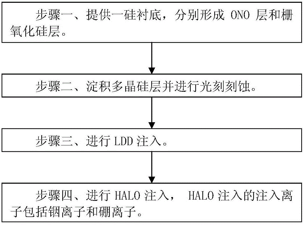
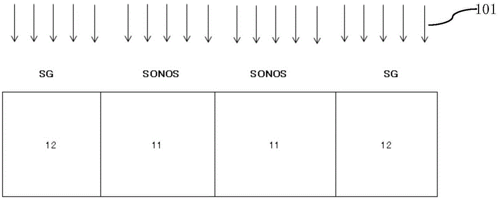
[0023] Such as figure 1 Shown is the flow chart of the method of the embodiment of the present invention; Figure 2A to Figure 2F As shown, it is a device structure diagram in each step of the method of the embodiment of the present invention; the unit structure of the SONOS device in the manufacturing method of the SONOS device of the embodiment of the present invention includes a memory cell tube 11 and a selection tube 12, such as Figure 2A The top of the storage cell tube 11 formation area is shown by SONOS, and the top of the selection tube 12 formation area is shown by SG; the manufacturing method of the cell structure of the SONOS device includes the following steps:

[0024] Step 1, such as Figure 2A As shown, a silicon substrate is provided, and a deep N well is implanted in the silicon substrate to form a deep N well, and the deep N well implantation is shown as 101 .

[0025] Such as Figure 2B As shown, a P-well implant and a threshold voltage (VT) adjustment ...


PUM


Abstract

The present invention discloses a manufacturing method of an SONOS device. A manufacturing method of a unit structure of the SONOS device comprises the following steps of providing a silicon substrate, and forming an ONO layer and a gate silicon oxide layer separately; depositing a polysilicon layer and carrying out the photoetching; carrying out the LDD injection; carrying out the HALO injection, wherein the injected ions comprise indium ions and boron ions. According to the present invention, by utilizing the characteristics that the indium ions are larger than the mass of the boron ions, are distributed shallowly after being injected, and are smaller in diffusion amount along with a heat process, and by adding the indium ion injection, the ion distribution of the HALO injection is adjusted, when the size of the SONOS device is reduced continuously, the ions of the HALO injection are distributed and concentrated at the bottom of a polysilicon gate by adding the indium ion injection, thereby being able to reduce the electric leakage of the SONOS device and the gate-induced drain electric leakage, facilitating reducing the size of the SONOS device, and being able to improve the reliability of the device.

Description

technical field [0001] The invention relates to a manufacturing process method of a semiconductor integrated circuit, in particular to a manufacturing method of a SONOS device. Background technique [0002] Non-volatile storage technology includes SONOS technology. During the programming or erasing process of the memory, due to the need to operate at high voltage, it often faces the problems of reducing leakage of storage devices, leakage and reliability of storage arrays under high-voltage application conditions. [0003] In the manufacturing process of the existing SONOS device, boron (Boron) ions are implanted as Halo to suppress the leakage between the source-drain (SD) junction. The continuous shrinking of the process size is the development trend of semiconductor integrated circuits. With the shrinking of the size, how to improve the device performance? Performance is a technical problem that constantly needs to be solved. Contents of the invention [0004] The tech...

Claims


Application Information

Patent Timeline
Patent Type & Authority Applications(China)
IPC IPC(8): H01L27/115H01L21/266
Inventor 熊伟张可钢陈华伦钱文生
Owner SHANGHAI HUAHONG GRACE SEMICON MFG CORP
Why Eureka
Try Eureka