Laser drilling and cutting system for semiconductor material

A laser drilling and cutting system technology, which is applied to semiconductor devices, laser welding equipment, circuits, etc., can solve the problems of inability to improve production efficiency, inability to solve manufacturing, and low efficiency of EDM technology

Active Publication Date: 2015-11-18
SHANGHAI MICRO SEMI WORLD
View PDF6 Cites 24 Cited by
  • Summary
  • Abstract
  • Description
  • Claims
  • Application Information

AI Technical Summary

Problems solved by technology

[0003] The traditional EDM technology has technical limitations such as extremely low efficiency in actual production, and the processed material needs to have good electrical conductivity, which cannot improve production efficiency.
The method of chemical etching cannot solve the problem of the manufacture of micropores with a diameter of less than 50 microns and a depth of more than 500 microns.
Therefore, the production of ...

Method used


Image

  • Laser drilling and cutting system for semiconductor material

Examples


Embodiment Construction

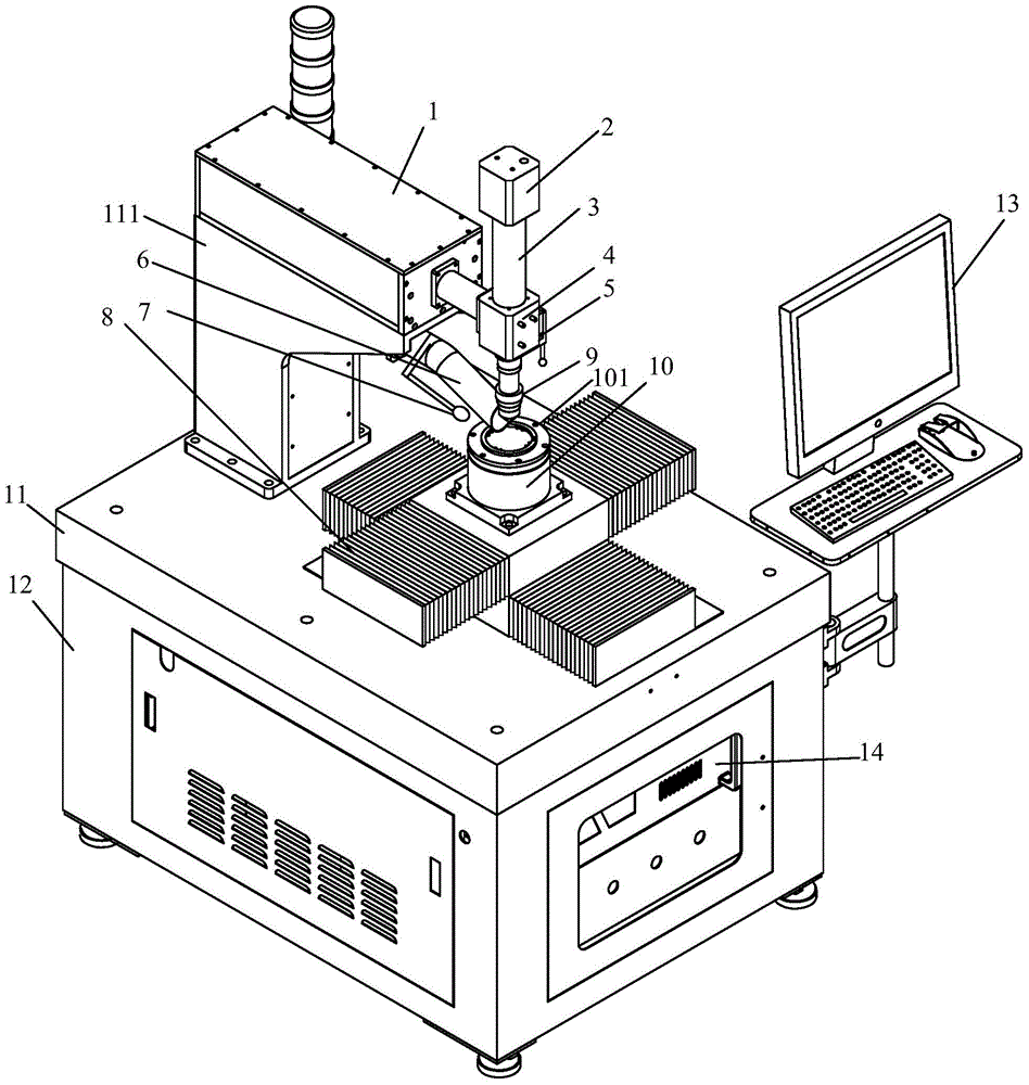
[0021] Such as figure 1 As shown, the laser drilling and cutting system for semiconductor materials of the present invention includes a base 12, a marble table 11, a laser optical path subsystem, a motion platform subsystem, a visual positioning detection subsystem and an industrial computer.

[0022] Wherein, the laser optical path subsystem is composed of a reflector 4 , a laser 1 arranged beside the reflector 4 , and a focusing mirror 9 arranged below the reflector 4 . The laser 1 is an infrared laser, preferably a fiber pulse laser.

[0023] The motion platform subsystem consists of an X / Y-axis superimposed motion platform 8 , a θ-axis rotating platform 10 and a Z-axis lifting adjustment mechanism 5 .

[0024] The marble countertop 11 is fixed on the base 12 , and the industrial computer 14 is located inside the base 12 . The X / Y-axis superimposed motion platform 8 is fixed on the marble table 11 , and the θ-axis rotating platform 10 is located on the X / Y-axis superimpos...


PUM


Abstract

The invention discloses a laser drilling and cutting system for a semiconductor material. The laser drilling and cutting system comprises a laser path subsystem, a motion platform subsystem, a vision positioning and detection subsystem and an industrial personal computer. The laser path subsystem is composed of a reflector, a laser unit arranged beside the reflector and a focusing mirror arranged below the reflector. The vision positioning and detection subsystem is composed of a displayer, an imaging lens cone, a camera, a focusing mirror and a lighting lamp. The imaging lens cone and the camera are located above the reflector on the same vertical line, the focusing mirror is located below the reflector, and the lighting lamp is arranged beside the focusing mirror. The camera is connected with the reflector through the imaging lens cone. The reflector can reflect lasers and also can conduct light transmittance of an imaging light source. Laser synchronous drilling, machine vision positioning secondary re-drilling, drilling form and position error detection, laser cutting and other functions are integrated and achieved for the semiconductor material in the motion process, and through hole and blind hole drilling, laser cutting, vision detection and other functions can be achieved for the semiconductor material in the motion process.

Description

technical field [0001] The invention belongs to the technical field of semiconductor material processing equipment, and in particular relates to a laser drilling and cutting equipment for semiconductor materials. Background technique [0002] With the advent of the information age, industries such as electronic information, communications, semiconductor integrated circuits, and high-power power electronics have developed rapidly, semiconductor materials have been widely used, and the demand is increasing. The through holes and blind holes of semiconductor materials are manufactured into chips. One of the core key processes of manufacturing, wafer manufacturing technology and processes require higher and higher manufacturing efficiency and positional accuracy for through holes and blinds. [0003] The traditional EDM technology has technical limitations such as extremely low efficiency in actual production, and the processed material needs to have good electrical conductivity...

Claims


Application Information

Patent Timeline
IPC IPC(8): B23K26/38B23K26/382B23K26/08B23K26/70B23K26/142B23K26/402B23K101/40
CPCB23K26/06B23K26/0823B23K26/0853B23K26/38B23K2101/40
Inventor 李轶徐伟涛丁波陈瀚侯金松杭海燕裴紫伟张杰蒋松
Owner SHANGHAI MICRO SEMI WORLD
Why Eureka
Try Eureka