Fin type field effect transistor formation method

A fin-type field effect transistor and fin technology, which is applied in electrical components, semiconductor/solid-state device manufacturing, circuits, etc., can solve problems such as fin damage, achieve damage prevention, good thickness consistency, and prevent adverse effects. Effect

Inactive Publication Date: 2015-11-25
SEMICON MFG INT (SHANGHAI) CORP
View PDF4 Cites 6 Cited by
  • Summary
  • Abstract
  • Description
  • Claims
  • Application Information

AI Technical Summary

Problems solved by technology

[0006] The problem solved by the present invention is to reduce the damage to the fin caused by the process of forming the shielding layer, and further reduce the consumption of fin materials while avoiding the damage to the fin caused by the process of forming a patterned photoresist layer

Method used


Image

  • Fin type field effect transistor formation method
  • Fin type field effect transistor formation method
  • Fin type field effect transistor formation method

Examples


Embodiment Construction

[0032] It can be seen from the background art that the performance of the fin field effect transistor formed in the prior art needs to be improved.

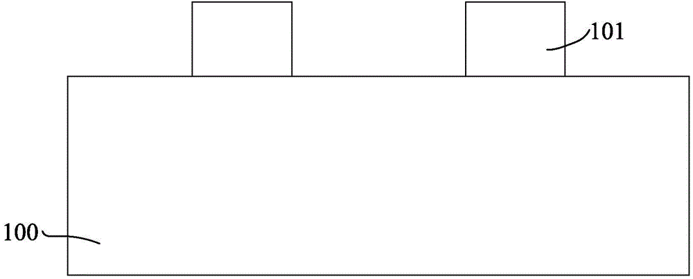
[0033] Research on the formation method of FinFETs found that after providing a substrate and forming several discrete fins on the substrate, it is usually necessary to perform ion implantation on the fins and doping the fins to improve the performance of FinFETs. Electrical properties, such as threshold voltage (Vt), saturation current (Idsat), etc.

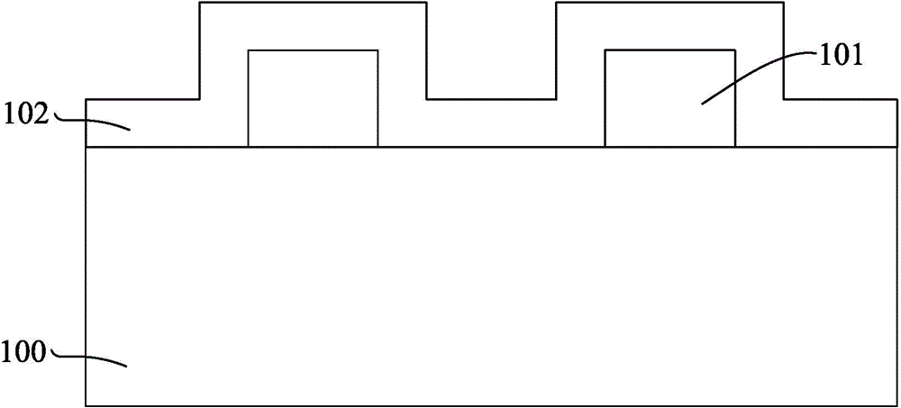
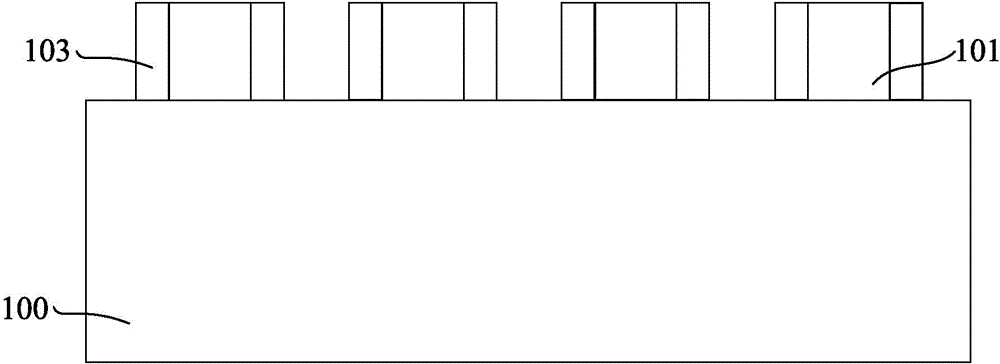
[0034] The process steps of doping the fins include: forming an initial photoresist layer covering the base and the surface of the fins; exposing the initial photoresist layer; The adhesive layer is cleaned to form a patterned photoresist layer, exposing part of the fins and the surface of the base; using the patterned photoresist layer as a mask, ion implantation is performed on the exposed fins.

[0035] However, the electrical performance of the fin field effect transistor form...


PUM


Abstract

The invention provides a fin type field effect transistor formation method comprising the steps that a substrate is provided, and multiple discrete fin parts are formed on the surface of the substrate; a shielding layer covering the surface of the fin parts is formed by adopting the deposition technology, and reactant gases of the deposition technology include a main source gas and an oxygen source gas, wherein the main source gas is gas including fin part material atoms; a photoresist film is formed on the surface of the shielding layer; exposure processing and development processing are performed on the photoresist film so that a patterned photoresist layer is formed; the patterned photoresist layer acts as a mask film, and the doping technology is performed on part of the fin parts; the patterned photoresist layer is removed; and the shielding layer is removed. In the technology process of formation of the shielding layer, consumption of the fin part material is low and even no fin part material is consumed so that the characteristic dimension of the fin parts is maintained to be unchanged. Besides, damage to the fin part material in the process of development processing can be prevented by the shielding layer so that the formed fin type field effect transistor is enabled to possess excellent electrical performance.

Description

technical field [0001] The invention relates to the technical field of semiconductor manufacturing, in particular to a method for forming a fin field effect transistor. Background technique [0002] With the continuous development of semiconductor process technology, the development trend of semiconductor process nodes following Moore's Law continues to decrease. In order to adapt to the reduction of process nodes, the channel length of MOSFET field effect transistors has to be continuously shortened. The shortening of the channel length has the advantages of increasing the die density of the chip and increasing the switching speed of the MOSFET field effect tube. [0003] However, as the channel length of the device is shortened, the distance between the source and the drain of the device is also shortened, so that the control ability of the gate to the channel becomes worse, and the gate voltage pinches off (pinchoff) the channel. The difficulty is also increasing, makin...

Claims


Application Information

Patent Timeline
Patent Type & Authority Applications(China)
IPC IPC(8): H01L21/336
Inventor 赵海虞肖鹏
Owner SEMICON MFG INT (SHANGHAI) CORP
Why Eureka
Try Eureka