
Integrated Fabry-Perot MEMS acceleration sensitive chip processing method

A technology for sensitive chips and processing methods, applied in metal processing equipment, metal processing machinery parts, manufacturing tools, etc., can solve problems such as damage and deformation of sensitive chips, and achieve the effects of ensuring consistency, high parallelism, and low difficulty in operation

Pending Publication Date: 2022-05-13
XI AN JIAOTONG UNIV
View PDF2 Cites 0 Cited by
  • Summary
  • Abstract
  • Description
  • Claims
  • Application Information

AI Technical Summary

Problems solved by technology

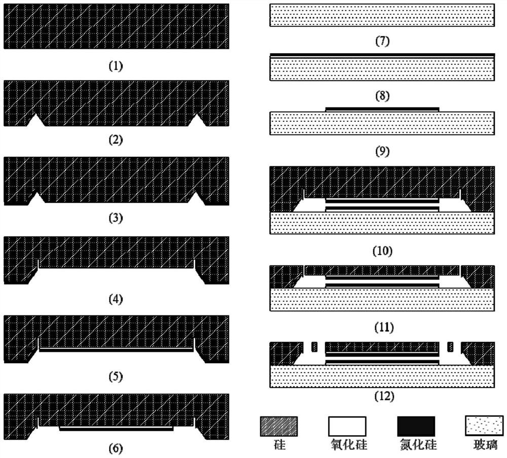
[0005] The purpose of the present invention is to provide an integrated Fabry-Perot MEMS acceleration-sensitive chip processing method to overcome the problem of deformation or damage of the sensitive chip caused by the residual stress in the prior art after etching first and then bonding, and has the advantages of simple process and high yield. In addition, the present invention can ensure that the cavity length of the final Fabry-Perot cavity is consistent with the design value, thereby ensuring that the sensor is in a highly sensitive working state

Method used


Image

  • Integrated Fabry-Perot MEMS acceleration sensitive chip processing method

Examples


Embodiment Construction

[0032] In order to make the purpose, technical solution and advantages of the present invention clearer, the technical solution of the present invention will be described in detail below. Apparently, the described embodiments are only some of the embodiments of the present invention, not all of them. Based on the embodiments of the present invention, all other implementations obtained by persons of ordinary skill in the art without making creative efforts fall within the protection scope of the present invention.

[0033] The following is combined with specific figure 1 The technical solution of the present invention is described in detail.

[0034] (1) Prepare a silicon wafer, first immerse it in acetone and alcohol solution for cleaning, and then immerse it in a solution of sulfuric acid / hydrogen peroxide for cleaning to remove oxide film, metal ions and other impurities.

[0035] (2) Utilizing the anisotropic wet etching technology of silicon to etch the silicon wafer cle...


PUM

PropertyMeasurementUnit
thicknessaaaaaaaaaa
thicknessaaaaaaaaaa
thicknessaaaaaaaaaa

Abstract

The invention discloses a method for processing an integrated Fabry-Perot MEMS acceleration sensitive chip, which comprises the following steps of: firstly, manufacturing a cavity depth reference groove by wet etching, etching a cavity on a silicon wafer by taking the groove as a reference, and repeatedly and alternately depositing silicon oxide and silicon nitride films on the surface of the cavity to manufacture an optical reflection increasing film; repeatedly and alternately depositing silicon oxide and silicon nitride films on the surface of the glass wafer, and patterning to form an optical reflection increasing film; carrying out anodic bonding on the silicon and the glass wafer, and thinning the silicon wafer to a target thickness; and finally, releasing the spring mass structure by adopting a deep reactive ion etching technology. According to the invention, the problem that the sensitive chip is deformed or damaged due to residual stress caused by bonding after etching in the prior art can be avoided, and the method has the advantages of simple process and high yield; in addition, due to the cavity depth reference groove step, it can be guaranteed that the manufactured sensitive chip works in a high-sensitivity state.

Description

technical field [0001] The invention relates to the technical field of micro-electro-mechanical systems, in particular to an integrated Fabry-Perot MEMS acceleration-sensitive chip processing method. Background technique [0002] MEMS acceleration sensors are widely used in robotics, drones, smart cars, consumer electronics and other fields due to their advantages of high precision, small size, low power consumption, low cost, and ease of mass production. At present, common MEMS acceleration sensors can be divided into capacitive, resonant, piezoresistive, optical and other types according to their different detection methods. Among them, the MEMS acceleration sensor based on the principle of optical interference combines the ultra-high displacement resolution of optical detection with the characteristics of small size and low power consumption of MEMS technology, and has a wide range of application prospects. [0003] The processing technology of the sensitive chip of the ...

Claims


Application Information

Patent Timeline
Patent Type & Authority Applications(China)
IPC IPC(8): B81C3/00B81C1/00
CPCB81C3/001B81C1/00468B81C1/00531B81C1/00539B81B2201/0235
Inventor 韦学勇赵明辉齐永宏李博蒋庄德
Owner XI AN JIAOTONG UNIV
Learn More