Forming method of semiconductor structure

A semiconductor and gate structure technology, which is applied in the field of semiconductor structure formation, can solve the problems of unstable leakage current performance, inhomogeneity, poor fin surface morphology and feature size, etc., and achieve the effect of precise and uniform structure size and avoiding damage

Active Publication Date: 2015-11-25
SEMICON MFG INT (SHANGHAI) CORP
View PDF4 Cites 15 Cited by
  • Summary
  • Abstract
  • Description
  • Claims
  • Application Information

AI Technical Summary

Problems solved by technology

[0005] However, in the existing fin field effect transistors, the surface morphology of the fins is poor, and the feature size (CD, Critical Dimension) is not uniform, which makes the fin field effect transistors prone to leakage current and unstable performance.

Method used


Image

  • Forming method of semiconductor structure
  • Forming method of semiconductor structure
  • Forming method of semiconductor structure

Examples


Embodiment Construction

[0034] As mentioned in the background, in the existing fin field effect transistors, the surface morphology of the fin portion is poor, and the feature size is not uniform.

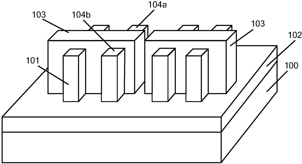
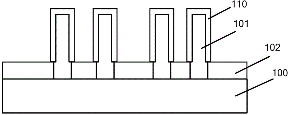
[0035] After research, it is found that in a process embodiment of forming a fin field effect transistor, such as figure 1 As shown, before the gate structure 103 is formed on the surface of the dielectric layer 102 and the top and sidewall surfaces of the fin 101, it is necessary to use an ion implantation process to dope P-type or N-type ions in the fin 101, so that the fin Portion 101 becomes an active region. In order to protect the fin 101 from damage during the ion implantation process, before the ion implantation process, a pad oxide layer 110 (such as figure 2 shown).

[0036]The thermal oxidation process is carried out in a high-temperature oxygen atmosphere, and by diffusing oxygen into the exposed sidewalls and top surfaces of the fins, the oxygen is combined with the semiconductor material ...


PUM

PropertyMeasurementUnit
thicknessaaaaaaaaaa

Abstract

A forming method of a semiconductor structure includes the steps: providing a substrate with fins on the surface, wherein the surface of the substrate and the surface of part of sidewalls of the fins are equipped with dielectric layers, and the surfaces of the dielectric layers are lower than the top surfaces of the fins; forming first protective layers on the surfaces of the dielectric layers, the surfaces of the sidewalls of the fins and the surfaces of the bottoms of the fins through a deposition technology, the density of the first protective layers being higher than the density of silicon oxide; forming second protective layers on the surfaces of the first protective layers through an oxidation technology; forming mask layers on the surfaces of the second protective layers, wherein the mask layers enable part of the second protective layers on the surfaces of the fins to be exposed, and the second protective layers are used for isolating the first protective layers from the mask layers; doping ions inside the fin through an ion implantation technology with the mask layers being masks; and removing the mask layers, the second protective layers and the first protective layers after the ion implantation, and exposing the surfaces of the dielectric layers, and part of the sidewalls and the bottom surfaces of the fins. A semiconductor structure formed through the method has a good shape, and has an accurate and uniform critical dimension.

Description

technical field [0001] The invention relates to the technical field of semiconductor manufacturing, in particular to a method for forming a semiconductor structure. Background technique [0002] With the rapid development of semiconductor manufacturing technology, semiconductor devices are developing towards higher element density and higher integration. As the most basic semiconductor device, transistors are currently being widely used. Therefore, with the increase of component density and integration of semiconductor devices, the gate size of planar transistors is getting shorter and shorter. The ability of traditional planar transistors to control channel current Weakened, resulting in short channel effect, resulting in leakage current, and ultimately affecting the electrical performance of semiconductor devices. [0003] In order to overcome the short-channel effect of the transistor and suppress the leakage current, a Fin Field Effect Transistor (FinFET) is proposed in...

Claims


Application Information

Patent Timeline
Patent Type & Authority Applications(China)
IPC IPC(8): H01L21/336H01L29/78
Inventor 赵海
Owner SEMICON MFG INT (SHANGHAI) CORP
Why Eureka
Try Eureka