
Test structure and test method for gate oxide integrity

A technology for testing structure and gate oxide layer, which is used in semiconductor/solid-state device testing/measurement, electrical components, electrical solid-state devices, etc., which can solve the problems of limited testing capability, long testing cycle time, and inability to guarantee test results.

Active Publication Date: 2015-11-25
SEMICON MFG INT (SHANGHAI) CORP
View PDF4 Cites 6 Cited by
  • Summary
  • Abstract
  • Description
  • Claims
  • Application Information

AI Technical Summary

Problems solved by technology

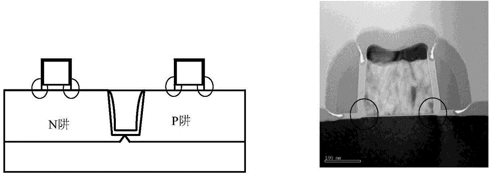
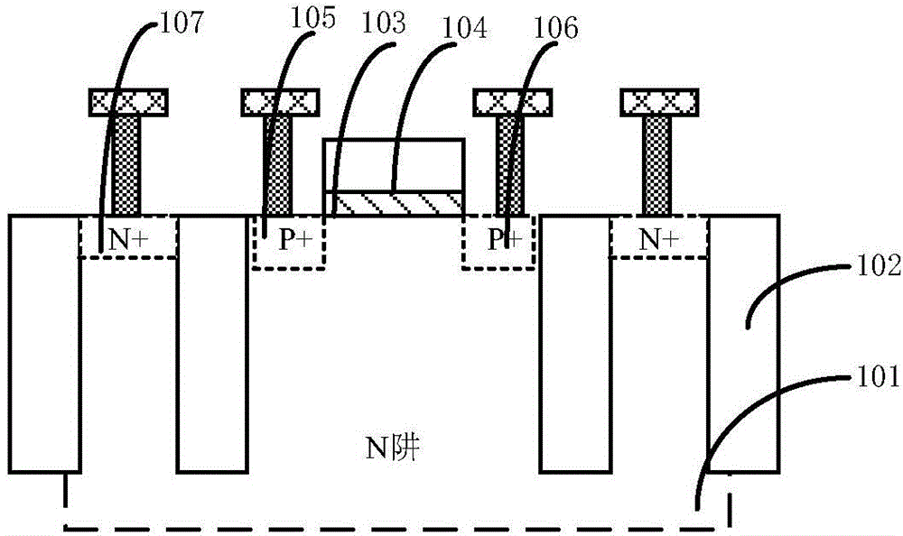
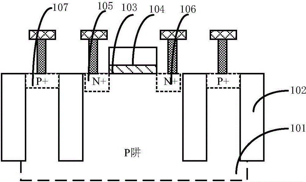
Although the test structure can accurately test the integrity of the gate oxide layer 103, the test structure and the test method need to consume a large amount of test cycle time. With the development of technology, the test capability of the test structure is limited. , but if the test cycle time is reduced, the test results cannot be guaranteed, so there is currently no way to reduce the test cycle time while ensuring that the test results are still acceptable

Method used


Image

  • Test structure and test method for gate oxide integrity
  • Test structure and test method for gate oxide integrity
  • Test structure and test method for gate oxide integrity

Examples


Embodiment 1

[0045] Attached below figure 2 The test structure of the present invention is further described.

[0046] First, the test structure includes at least:

[0047] A semiconductor substrate 201, in which an N well and a P well are arranged at intervals;

[0048] a gate structure, including a gate oxide layer 203 and a gate electrode 204, the gate structure is partially located above the N well and partially above the P well;

[0049] a source region and a drain region respectively located in the N well and the P well on both sides of the gate structure;

[0050] Wherein the semiconductor substrate 201 , the source region and the drain region are grounded, and the gate structure is connected to a power supply voltage.

[0051] Wherein, the semiconductor substrate 201 may be at least one of the materials mentioned below: silicon, SiGe, etc., and other active devices may also be formed in the semiconductor substrate. A silicon substrate is preferred in the present invention.

...

Embodiment 2

[0072] The present invention also provides a method for testing the test structure prepared in Example 1, the method includes applying a gradually increasing stress voltage on the gate structure to measure the breakdown voltage of the gate oxide layer , and then evaluate the gate oxide layer.

[0073] In this embodiment, the breakdown voltage of the gate oxide layer is tested by a ramp voltage test method. The Vramp test ramps up the acceleration voltage linearly from the operating voltage to the breakdown of the oxide layer. According to the measured breakdown voltage, the The gate oxide layer is evaluated. If the measured breakdown voltage is higher than the specified voltage, it means that there are no defects in the gate oxide layer and the edge of the gate structure; if the measured breakdown voltage is lower than If the specified voltage is higher, it indicates that there are defects in the gate oxide layer and the edge of the gate structure.

[0074] In the method, the...


PUM


Abstract

The invention relates to a test structure and a test method for gate oxide integrity. The test structure comprises the components of a semiconductor substrate on which an N well and a P well are separately formed; a gate electrode structure which comprises a gate oxide and a gate electrode, wherein the gate structure is partially arranged above the N well and is partially arranged above the P well; and a source region and a drain region which are respectively arranged in the N well and the P well at two sides of the gate electrode structure, wherein a gradually increased stress voltage is applied on the gate electrode structure. The test structure can effectively evaluate device damage of the gate electrode in a patterning process. Not only is detecting efficiency improved, but also the area of the test structure can be further reduced.

Description

technical field [0001] The invention relates to a semiconductor manufacturing process, and in particular, the invention relates to a test structure and a test method for the integrity of a gate oxide layer. Background technique [0002] With the continuous development of technology, the thickness of the gate oxide layer of integrated circuits is also reduced from 20-30nm to less than 1nm. The gate oxide layer continues to develop towards the film direction, but the power supply voltage should not be lowered. At higher electric field strengths, the performance of the gate oxide is bound to become a prominent issue. [0003] Poor electrical resistance of gate oxide will cause unstable electrical parameters of MOS devices, such as: threshold voltage drift, transconductance drop, leakage current increase, etc., which will further cause gate oxide breakdown, resulting in device failure and causing the entire integrated circuit to fall into paralyzed state. Therefore, the break...

Claims


Application Information

Patent Timeline
Patent Type & Authority Applications(China)
IPC IPC(8): H01L23/544H01L21/66
Inventor 许晓锋宋永梁
Owner SEMICON MFG INT (SHANGHAI) CORP
Learn More