Dispersion method for nanometer silicon
A technology of nano-silicon and nano-silica powder, which is applied in the treatment of dyed polymer organic compounds, electrical components, battery electrodes, etc., can solve the problems of unsatisfactory effect, unreasonable molecular structure design, unsatisfactory dispersion and stabilization effect, etc. problem, to achieve the effect of simple and effective structure, improvement of agglomeration problems, and simple structure
- Summary
- Abstract
- Description
- Claims
- Application Information
AI Technical Summary
Problems solved by technology
Method used
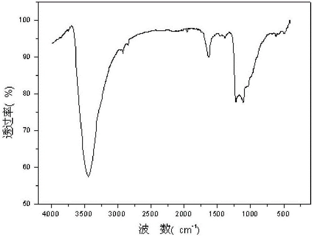
Image

Examples
Embodiment 1
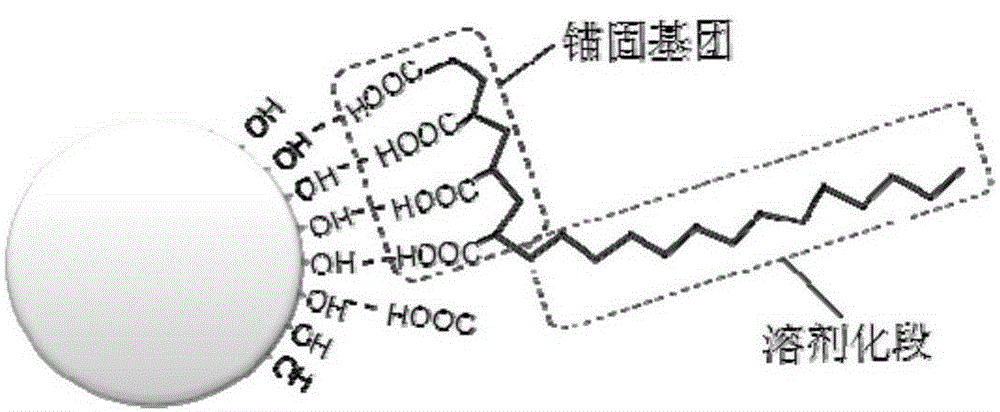
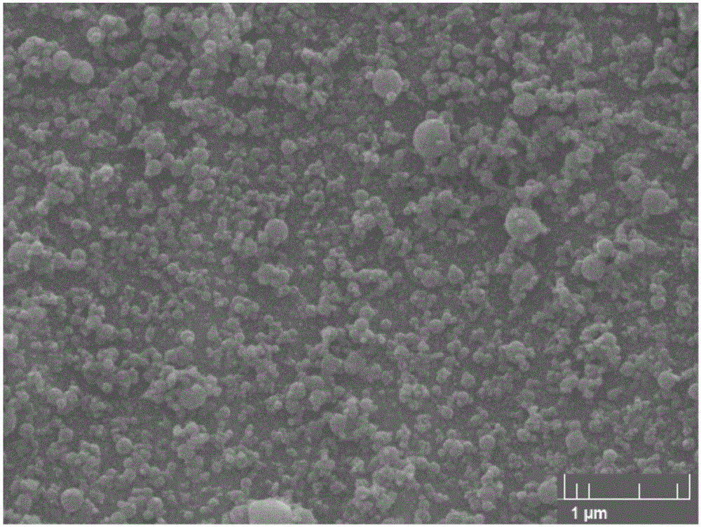
[0038] A method for dispersing nano-silicon of the present invention, comprising the following steps: adding nano-silicon powder (severe agglomeration, average particle is about 80nm) produced by Guilin Institute of Mineral Geology into pure water and stirred evenly to form a solid content of 1% placed in an ultrasonic cleaner to control the water temperature at 20-30°C and disperse for 20 minutes under the condition of ultrasonic power of 300w, and then add polyether hyperdispersants with multi-anchor groups (molecular weight: 2000 ), using mechanical stirring for 6h to obtain a uniformly dispersed nano-silicon dispersion. The measured particle size of the nano-silicon dispersion is 191nm; image 3 as shown,
[0039] The particle size of the nano-silicon dispersion prepared in this example was sealed and left for 15 days and measured to be 207 nm, and then placed in a constant temperature water bath at 80° C. for 40 hours, and the particle size was measured to be 201 nm.
...
Embodiment 2
[0044] A method for dispersing nano-silicon of the present invention, comprising the following steps: adding nano-silicon powder (severe agglomeration, average particle is about 80nm) produced by Guilin Institute of Mineral Geology into pure water and stirred evenly to form a solid content of 1% Using a high-speed disperser to disperse at a speed of 30,000r / min for 20 minutes, then add a multi-anchor group polyether hyperdispersant (molecular weight: 2000) with 10% of the mass of silicon powder, and use mechanical stirring for 6 hours to obtain a uniformly dispersed nano-silicon liquid. Silicon dispersion. The particle size of the nano-silicon dispersion was measured to be 233nm; the particle size of the nano-silicon dispersion was measured to be 231nm after being sealed and left to stand for 15 days.
Embodiment 3
[0048] A method for dispersing nano-silicon of the present invention, comprising the following steps: adding nano-silicon powder (severe agglomeration, average particle is about 80nm) produced by Guilin Institute of Mineral Geology into pure water and stirred evenly to form a solid content of 5% placed in an ultrasonic cleaner to control the water temperature to 20-30°C and disperse for 20 minutes under the condition of an ultrasonic power of 300w, and then add a multi-anchor group polyether hyperdispersant (molecular weight: 2000 ), using mechanical stirring for 6h to obtain a uniformly dispersed nano-silicon dispersion. The particle size of the nano-silicon dispersion was measured to be 223nm. The particle size was measured to be 231nm after being sealed and left for 15 days, and the particle size was measured to be 229nm after being placed in a constant temperature water bath at 80°C for 40 hours.
PUM
| Property | Measurement | Unit |
|---|---|---|
| Granularity | aaaaa | aaaaa |
| Granularity | aaaaa | aaaaa |
| Granularity | aaaaa | aaaaa |
Abstract
Description
Claims
Application Information