A three-dimensional silicon-based micro-nano photonic crystal solar cell

A technology of solar cells and micro-nano photons, applied in the field of solar cells, can solve the problems of surface reflection loss, complex production process, narrow reflection band, etc., to reduce equivalent grid electrode resistance, improve photoelectric conversion efficiency, and strong light trapping ability Effect

Active Publication Date: 2019-05-10
QINGDAO UNIV
View PDF1 Cites 0 Cited by
  • Summary
  • Abstract
  • Description
  • Claims
  • Application Information

AI Technical Summary

Problems solved by technology

Studies have shown that only by adopting a light-trapping structure can the photoelectric conversion efficiency of the battery be guaranteed. In addition to reducing the reflection of the light-incoming surface of the battery and minimizing the coverage area of ​​the front electrode, the existing light-trapping method is mainly to increase the light after the light enters the battery body. The path of light in the absorbing layer makes the refractive index of the absorbing layer greater than that of the upper and lower texture materials, so that the unabsorbed light returns to the battery absorbing layer again for secondary or multiple absorption, such as using a single-layer or multi-layer anti-reflection film , depositing a layer of anti-reflection film with gradually changing refractive index on the silicon surface, or combining anti-reflection film technology with surface texturing technology to prepare anti-reflection film with textured structure, etc., but these technologies have a narrow reflection band , the preparation process is difficult to control and other deficiencies, most of the research is in the experimental stage
[0004] Recently, studies have suggested that silicon nanowires (or pores) may be one of the most potential, low-cost, and high-efficiency solar cell device materials. Silicon nanowires can increase light absorption, but most of the existing research is on nanoscale solar cell structures with one-dimensional structures. , the mechanism used is to trap light through diffuse reflection. Some studies have proposed a two-dimensional structure of radial silicon nanowires, but its fabrication process is complicated, and it has not been combined with the forbidden band and slow light theory of photonic crystal structure.
Chinese patent ZL201410504341.2 discloses a two-dimensional silicon-based micro-nano photonic crystal solar cell, and ZL20151019657.5 discloses a two-dimensional silicon-based photonic crystal solar cell. These two two-dimensional silicon-based solar cell structures have photon-forbidden With the advantages of slow light effect, small thickness, good light trapping, and high photoelectric conversion efficiency, the core part of silicon-based solar cells is the PN junction. The photovoltaic effect of the PN junction converts solar energy into electrical energy. If the wire is connected to the load , can generate direct current in the circuit. In the actual work of solar cells, the main factors affecting the efficiency of solar cells can be attributed to two aspects, optical loss and electrical loss. The most important factor is optical absorption. The main influencing factors are: (1) The loss of surface reflection; (2) The battery body cannot trap light well, and the light cannot be fully absorbed when it is incident; (3) The coverage area of ​​the electrode material on the light-incoming surface loses the total energy of the incident light, etc.; resulting in electrical The influencing factors of the loss are: (1) the coincident lifetime of photogenerated carriers; (2) the directional mobility of photogenerated carriers is not strong; (3) the influence of structural equivalent series resistance, in existing solar cells, this Both effects can cause a battery to lose nearly 70% of its energy

Method used


Image

  • A three-dimensional silicon-based micro-nano photonic crystal solar cell
  • A three-dimensional silicon-based micro-nano photonic crystal solar cell
  • A three-dimensional silicon-based micro-nano photonic crystal solar cell

Examples


Embodiment 1

[0038] Example 1: Line-defect waveguide with triangular lattice arrangement

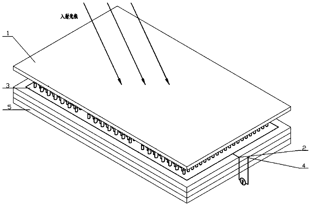
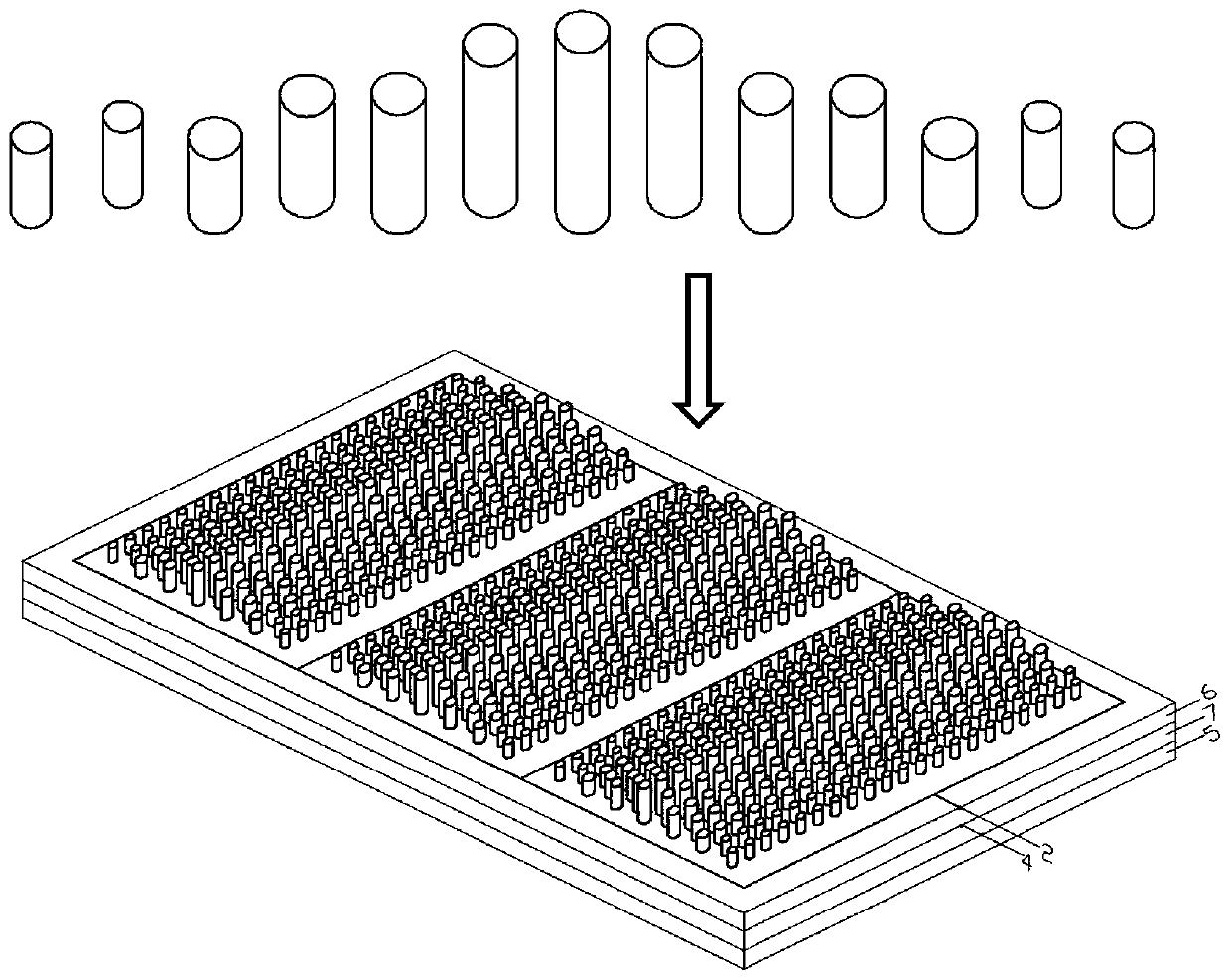
[0039] The overall structure of this embodiment is as figure 1 As shown, FIG. 2 is a schematic diagram of the three-dimensional silicon-based micro-nano photonic crystal solar cell structure 3 described in this embodiment, wherein the n-type silicon semiconductor 6 is a structure with a periodic arrangement of two substructures with a forbidden band and a slow light effect:

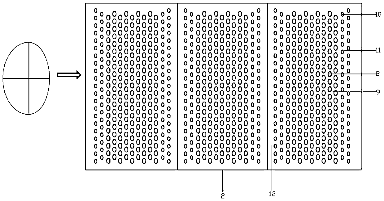
[0040] (1) Forbidden zone: The forbidden zone scattering element 8 of the n-type silicon semiconductor 6 adopts an asymmetric elliptical scattering element (the long axis of the structure is the same, the short axis is different, e will have 2 different values), and the spatial arrangement is triangular Lattice structure; the central wavelength of forbidden band is set at λ=700nm, can obtain by plane wave expansion method: when the central wavelength of forbidden band is set at 700nm, the lattice constant of n-type silicon semic...

Embodiment 2

[0044] Example 2: Reticulate line defect waveguide arranged in a quadrilateral

[0045] The overall structure of this embodiment and figure 1 Similarly, Fig. 5 is a schematic diagram of a three-dimensional silicon-based micro-nano photonic crystal solar cell structure 3, wherein the n-type silicon semiconductor 6 is a structure with a periodic arrangement of two substructures with a band gap and a slow light effect:

[0046] (1) band gap: the band gap scattering element 8 of the n-type silicon semiconductor 6 adopts a symmetrical circular bow-shaped scattering element, and the space is arranged as a symmetrical structure of a four-sided lattice; the central wavelength of the band gap is set at λ=700nm, by Plane wave expansion method can obtain: when the central wavelength of forbidden band is set at 700nm, the lattice constant of n-type silicon semiconductor 6 is a=0.29λ, the major axis parameter b=0.40a, e=0.28 of scattering element 8 in forbidden band region ; The height h ...


PUM


Abstract

The invention belongs to the technical field of solar cells and relates to a three-dimensional silicon-based micro-nano photonic crystal solar cell. The three-dimensional silicon-based micro-nano photonic crystal solar cell is characterized in that a front electrode is arranged on the lower surface of a front contact layer, a three-dimensional silicon-based micro-nano photonic crystal solar cell structure is arranged between the front electrode and a back electrode, an upper layer of the three-dimensional silicon-based micro-nano photonic crystal solar cell structure is an n-type silicon semiconductor layer while a lower layer thereof is a p-type silicon semiconductor layer, the front electrode is embedded into the bottom of a line defect waveguide of the n-type silicon semiconductor layer, the p-type silicon semiconductor layer can form a plane with the back electrode, a back contact layer is arranged at the bottom of the back electrode, and the back electrode is arranged in a slow light region or a forbidden band region of the p-type silicon semiconductor layer. The three-dimensional silicon-based micro-nano photonic crystal solar cell has the advantages of small thickness, material saving, short current carrier diffusion distance, high stability, high transmission efficiency, there-dimensional structure regularity, flexibility and mature processing and compositing techniques, and therefore can be developed as a new-generation low-cost efficient solar cell device with the highest potential.

Description

Technical field: [0001] The invention belongs to the technical field of solar cells, and relates to a novel photonic crystal solar cell structure, in particular to a high-efficiency photonic crystal solar cell structure that makes full use of light, organically combines light trapping with photon band gap and slow light effect, has high photoelectric conversion efficiency, and saves materials. Three-dimensional silicon-based micro-nano photonic crystal solar cells. Background technique: [0002] A solar cell is a semiconductor device that converts light energy into electrical energy, and is an important form of solar energy utilization. Although there are many types of solar cells according to the base material, silicon-based solar cells are widely used at present because silicon is rich in raw materials, high in photoelectric conversion efficiency, high in stability and reliability of photoelectric performance, and mature processing technology. It is determined by factors ...

Claims


Application Information

Patent Timeline
Patent Type & Authority Patents(China)
IPC IPC(8): H01L31/068H01L31/0352
CPCH01L31/035227H01L31/068Y02E10/547
Inventor 万勇高竞徐胜姜澄溢刘浩楠
Owner QINGDAO UNIV
Why Eureka
Try Eureka