Organic thin film transistor array substrate and manufacturing method therefor

A transistor array and fabrication method technology, applied in semiconductor/solid-state device manufacturing, electrical solid-state devices, semiconductor devices, etc., can solve problems such as reducing conduction capacity, affecting quality, and reducing, reducing the number of processes and improving production efficiency. Effect

Active Publication Date: 2015-12-09
SHENZHEN CHINA STAR OPTOELECTRONICS TECH CO LTD
View PDF4 Cites 6 Cited by
  • Summary
  • Abstract
  • Description
  • Claims
  • Application Information

AI Technical Summary

Problems solved by technology

In addition, the electrode material of the current OTFT generally chooses silver (Ag), a metal material with a low work function, to reduce the contact resistance, but Ag is easily oxidized without a protective layer to reduce the conductivity.
[0004] In view of the above problems, the present invention proposes a new manufacturing method for OTFT array substrates, which not only reduces the number of times of photomask, lithography, and etching processes required in the overall manufacturing process, but also protects the electrodes of the metal layer, such as silver electrodes, from Oxidation occurs in subsequent processes, which affects the quality of devices made of OTFT array substrates

Method used


Image

  • Organic thin film transistor array substrate and manufacturing method therefor
  • Organic thin film transistor array substrate and manufacturing method therefor
  • Organic thin film transistor array substrate and manufacturing method therefor

Examples


Embodiment Construction

[0043] The word "embodiment" as used in this specification means an example, instance or illustration. Furthermore, as used in this specification and the appended claims, the article "a" or "an" may generally be construed as "one or more" unless specified otherwise or clear from the context in the singular. The following descriptions of the various embodiments refer to the accompanying drawings to illustrate specific embodiments in which the present invention can be practiced. The directional terms mentioned in the present invention, such as "up", "down", "front", "back", "left", "right", "inside", "outside", "side", etc., are for reference only The orientation of the attached schema. Therefore, the directional terms used are used to illustrate and understand the present invention, but not to limit the present invention.

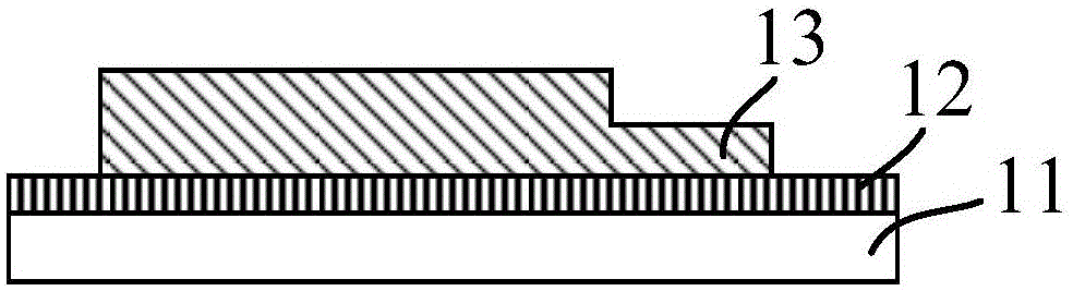
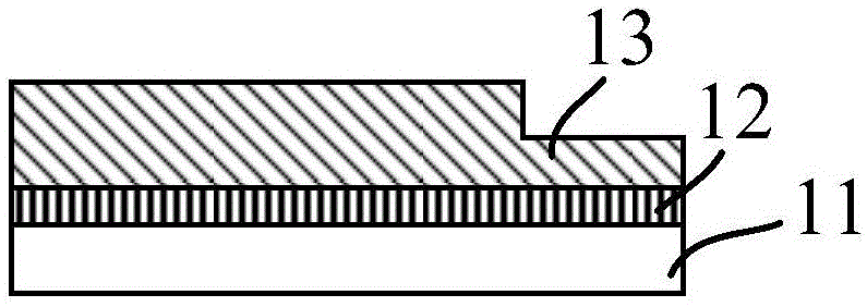
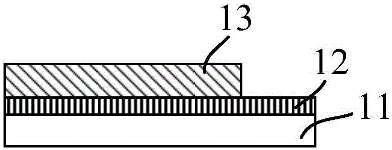
[0044] The present invention proposes a manufacturing process of an organic thin film transistor array substrate, which roughly includes the following pro...


PUM


Abstract

The invention discloses an organic thin film transistor array substrate and a manufacturing method therefor. The manufacturing method comprises: continuously depositing on a substrate to form a metal layer thin film, then depositing an indium tin oxide (ITO) layer, coating a photoresist layer to form source and drain patterns, a data line and an anode of a pixel electrode simultaneously after a first manufacturing process for a mask, then manufacturing an organic semiconductor layer, an organic insulation layer, a gate electrode, a scanning line and a passivation layer in sequence, finally digging the covered passivation layer in the position of the pixel electrode (namely the OLED anode) to expose the electrode at the bottom layer, and then plating an OLED material layer on the exposed ITO pixel electrode to form an OLED device.

Description

【Technical field】 [0001] The invention relates to the field of display technology, in particular to an organic thin film transistor array substrate and a manufacturing method thereof. 【Background technique】 [0002] Organic thin film transistor (OrganicThinFilmTransistor, OTFT) is a thin film transistor made of organic matter as a semiconductor material. OTFT can be produced at low temperature or normal temperature, so the substrate of OTFT can be replaced by lighter, thinner and cheaper plastic instead of glass. Compared with traditional inorganic thin-film transistors, OTFT is simpler to manufacture, and has lower requirements on the conditions and purity of the film-forming environment, so its manufacturing cost is relatively low, and its simple process characteristics and excellent flexibility have greatly improved its application in many fields. It can be applied to flexible display, electronic skin, flexible sensor and other fields. [0003] In the conventional fabric...

Claims


Application Information

Patent Timeline
Patent Type & Authority Applications(China)
IPC IPC(8): H01L21/77H01L27/12
CPCH01L27/1214H01L27/124H01L27/1259G02F1/1368H10K59/00H10K99/00
Inventor 徐洪远
Owner SHENZHEN CHINA STAR OPTOELECTRONICS TECH CO LTD
Why Eureka
Try Eureka