Method for improving carrier transmission efficiency of backside illumination image sensor

An image sensor and transmission efficiency technology, which is applied in the field of image sensors, can solve the problems of affecting control flexibility, difficulty in free adjustment of step potential difference, and limitation of carrier transmission efficiency, so as to achieve the effect of improving response speed and image quality

Inactive Publication Date: 2015-12-16
GALAXYCORE SHANGHAI
View PDF5 Cites 10 Cited by
  • Summary
  • Abstract
  • Description
  • Claims
  • Application Information

AI Technical Summary

Problems solved by technology

However, in this application, the non-uniformly doped polysilicon gate is controlled as a whole by the same voltage signal, so that the potentials of the channel regions under different types of doped regions increase or decrease at the same time, so it is difficult to freely adjust the step potentials. The difference affects the control flexibility and limits the improvement of carrier transport efficiency

Method used


Image

  • Method for improving carrier transmission efficiency of backside illumination image sensor
  • Method for improving carrier transmission efficiency of backside illumination image sensor
  • Method for improving carrier transmission efficiency of backside illumination image sensor

Examples


Embodiment 1

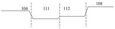
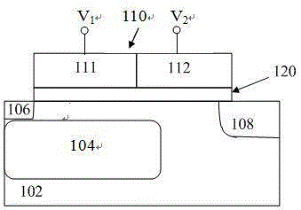
[0030] FIG. 1( a ) is a schematic structural diagram of a transfer transistor in a CMOS image sensor according to an embodiment of the present application. Wherein, the P-type substrate 102 may be a semiconductor substrate, or may include a semiconductor substrate and an epitaxial layer laid thereon, and the material of the semiconductor substrate may be a common semiconductor substrate material such as silicon, germanium, and gallium arsenide. A carrier collection region 104 with N-type doping is formed in the P-type substrate 102 to form a photodiode, which receives light incident from the bottom of the image sensor and generates photogenerated carriers. In this embodiment, the carriers are electrons. The carrier collection region 104 of the photodiode acts as the source of the transfer transistor. In addition, a floating diffusion region 108 with N-type doping is formed in the P-type substrate 102 , and the floating diffusion region 108 serves as the drain of the transfer ...

Embodiment 2

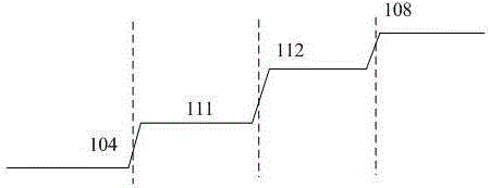
[0039] FIG. 2( a ) is a schematic structural diagram of a transfer transistor in a CMOS image sensor according to another embodiment of the present application. Wherein, the P-type substrate 102 may be a semiconductor substrate, or may include a semiconductor substrate and an epitaxial layer laid thereon, and the material of the semiconductor substrate may be a common semiconductor substrate material such as silicon, germanium, and gallium arsenide. A carrier collection region 104 with N-type doping is formed in the P-type substrate 102 to form a photodiode, which receives light incident from the bottom of the image sensor and generates photogenerated carriers. In this embodiment, the carriers are electrons. The carrier collection region 104 of the photodiode acts as the source of the transfer transistor. In addition, a floating diffusion region 108 with N-type doping is formed in the P-type substrate 102 , and the floating diffusion region 108 serves as the drain of the tran...

Embodiment 3

[0048] FIG. 3( a ) shows a schematic structural diagram of a transfer transistor in a CMOS image sensor according to another embodiment of the present application. Wherein, the P-type substrate 102 may be a semiconductor substrate, or may include a semiconductor substrate and an epitaxial layer laid thereon, and the material of the semiconductor substrate may be a common semiconductor substrate material such as silicon, germanium, and gallium arsenide. A carrier collection region 104 with N-type doping is formed in the P-type substrate 102 to form a photodiode, which receives light incident from the bottom of the image sensor and generates photogenerated carriers. In this embodiment, the carriers are electrons. The carrier collection region 104 of the photodiode acts as the source of the transfer transistor. In addition, a floating diffusion region 108 with N-type doping is formed in the P-type substrate 102 , and the floating diffusion region 108 serves as the drain of the t...


PUM


Abstract

The invention provides a method for improving the carrier transmission efficiency of a backside illumination image sensor. The method comprises the following steps of: forming a photodiode and a floating diffusion region; forming a transfer transistor, wherein the source electrode of the transfer transistor is a carrier collecting region of the photodiode, the drain electrode of the transfer transistor is the floating diffusion region, the polycrystalline silicon gate electrode of the transfer transistor successively comprises, along the direction from the source electrode to the drain electrode of the transfer transistor, a P-type doped gate region and an N-type doped gate region, the P-type doped gate region at least partially covers the carrier collecting region of the photodiode, and the N-type doped gate region at least partially covers the channel region of the transfer transistor; applying a first voltage signal to the P-type doped gate region and applying a second voltage signal to the N-type doped gate region in order that the potential in the channel region is distributed in a stepped manner so as to improve the transmission efficiency of the carriers from the photodiode to the floating diffusion region, wherein the first voltage signal is not higher than the second voltage signal.

Description

technical field [0001] The invention relates to the field of image sensors, in particular to a method for improving carrier transmission efficiency of a back-illuminated image sensor. Background technique [0002] Compared with the manufacturing process of CCD, the manufacturing process of CMOS image sensor is compatible with the standard CMOS process, and has the characteristics of low power consumption, easy integration, and low cost. Therefore, CMOS image sensor is more and more widely used in various electronic devices middle. The structures of active pixels in a CMOS image sensor can be classified into different types according to the number of transistors. A typical 4-T active pixel is shown in Figure 1, including photodiode (photodiode, PD), transfer transistor (transfertransistor, TX), floating diffusion (floating diffusion, FD), reset transistor (resettransistor, RST), select transistor (selecttransistor, SEL). [0003] Traditional CMOS image sensors use front si...

Claims


Application Information

Patent Timeline
Patent Type & Authority Applications(China)
IPC IPC(8): H01L21/8238H01L27/146H01L29/36H01L29/423
CPCH01L27/14687H01L27/14632H01L27/1464H01L29/36H01L29/4232
Inventor 李杰
Owner GALAXYCORE SHANGHAI
Why Eureka
Try Eureka