Silicon carbide metal-oxide-semiconductor field-effect-transistor (MOSFET) device and fabrication method thereof

A production method and technology of silicon carbide, applied in semiconductor/solid-state device manufacturing, semiconductor devices, electrical components, etc., can solve the problems of strict polysilicon thermal oxidation process requirements, channel size cannot be precisely controlled, etc., to avoid avalanche strikes wear, good conduction characteristics, and the effect of avoiding false opening

Active Publication Date: 2015-12-16
INST OF MICROELECTRONICS CHINESE ACAD OF SCI +1
View PDF3 Cites 19 Cited by
  • Summary
  • Abstract
  • Description
  • Claims
  • Application Information

AI Technical Summary

Problems solved by technology

This method has strict requirements on the thermal oxidation process of polysilicon, and the size of the formed channel cannot be precisely controlled

Method used


Image

  • Silicon carbide metal-oxide-semiconductor field-effect-transistor (MOSFET) device and fabrication method thereof
  • Silicon carbide metal-oxide-semiconductor field-effect-transistor (MOSFET) device and fabrication method thereof
  • Silicon carbide metal-oxide-semiconductor field-effect-transistor (MOSFET) device and fabrication method thereof

Examples


Embodiment Construction

[0048] In order to make the object, technical solution and advantages of the present invention clearer, the present invention will be further described in detail below in conjunction with specific embodiments and with reference to the accompanying drawings.

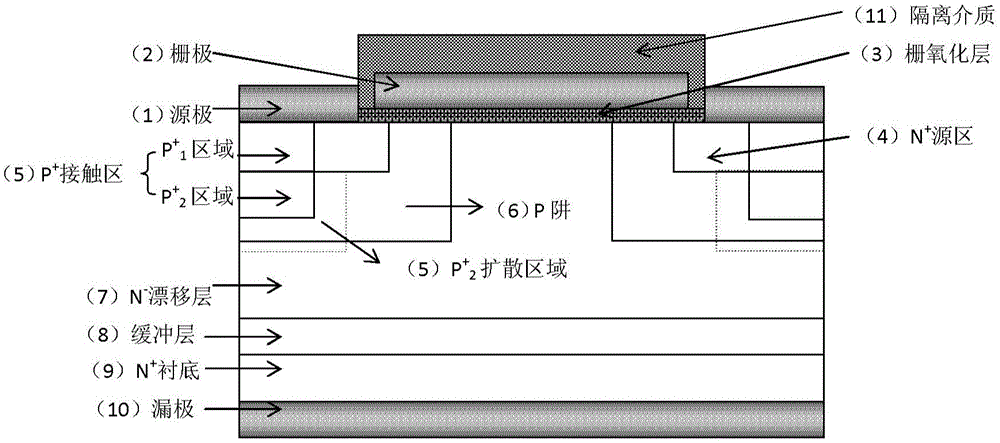
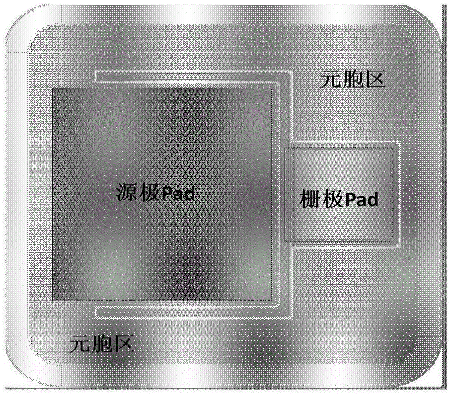
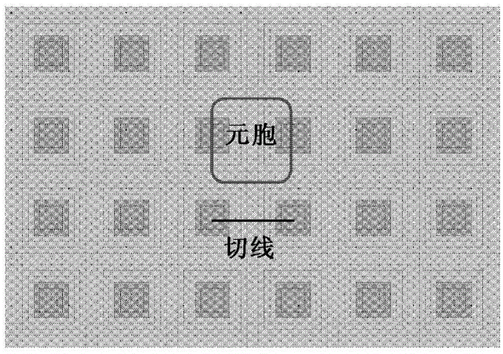
[0049] In the self-aligned silicon carbide MOSFET device provided by the present invention, the self-aligned silicon carbide MOSFET device is composed of a plurality of silicon carbide MOSFET device cells connected in parallel, and the silicon carbide MOSFET device cells are uniformly arranged. Figure 1a It shows a schematic structural diagram of a single self-aligned silicon carbide MOSFET device cell according to an embodiment of the present invention, Figure 1b is a layout for making a single self-aligned silicon carbide MOSFET device according to an embodiment of the present invention, Figure 1c yes Figure 1b A schematic diagram of a cell area in a device layout, Figure 1c The solid line box is defined as a cel...


PUM

PropertyMeasurementUnit
thicknessaaaaaaaaaa

Abstract

The invention discloses a self-aligned silicon carbide metal-oxide-semiconductor field-effect-transistor (MOSFET) device with an optimized P<+> region and a fabrication method of the self-aligned silicon carbide MOSFET device. The self-aligned silicon carbide MOSFET device is formed by connecting a plurality of same cells in parallel, and the cells of the silicon carbide MOSFET device are uniformly arranged. Each cell of the silicon carbide MOSFET device comprises two sources, a grid, a grid oxide layer, two N<+> source regions, two P<+> contact regions, two P pits, an N<-> drift layer, a buffer layer, an N<+> substrate, a drain and an isolation dielectric layer. By optimizing the P<+> region, favorable source ohmic contact is formed, the on resistance is reduced, meanwhile, the source and the P pits are in short connection, parasitic negative-positive-negative (PNP) and a parasitic transistor effect of PiN are prevented, the conduction property and the breakdown property of the device can be compatible, and the device can be used in a high-voltage and high-frequency silicon carbide MOSFET device. A self-aligned fabrication method is adopted by the invention, the process is simplified, the channel size is accurately controlled, and a transverse or longitudinal power MOSFET can be fabricated.

Description

technical field [0001] The invention relates to a self-aligned silicon carbide MOSFET device and its manufacturing process, in particular to an optimized P + Area self-aligned silicon carbide MOSFET devices and methods of fabrication thereof. Background technique [0002] Silicon carbide material has excellent physical and electrical properties. With its unique advantages such as wide band gap, high thermal conductivity, large saturation drift velocity and high critical breakdown electric field, it has become a high-power, high-frequency, high-voltage It is an ideal semiconductor material for high temperature resistant and radiation resistant devices, and has broad application prospects in military and civil affairs. Silicon carbide MOSFET devices have the advantages of fast switching speed and small on-resistance, and can achieve a high breakdown voltage level at a small drift layer thickness, reduce the volume of the power switch module, and reduce energy consumption. , ...

Claims


Application Information

Patent Timeline
Patent Type & Authority Applications(China)
IPC IPC(8): H01L29/78H01L29/06H01L21/04
CPCH01L21/0445H01L29/0696H01L29/66068H01L29/7802H01L29/7803
Inventor 汤益丹申华军白云周静涛杨成樾刘新宇李诚瞻刘国友
Owner INST OF MICROELECTRONICS CHINESE ACAD OF SCI
Why Eureka
Try Eureka