A kind of memristor based on fiber substrate and preparation method thereof

A fiber substrate and memristor technology, applied in electrical components and other directions, can solve the problems of high cost and inflexibility, and achieve the effects of low cost, easy extraction and light weight

Active Publication Date: 2019-04-09
CENT SOUTH UNIV
View PDF5 Cites 0 Cited by
  • Summary
  • Abstract
  • Description
  • Claims
  • Application Information

AI Technical Summary

Problems solved by technology

[0007] In view of the disadvantages of memristor devices in the prior art, such as inflexibility and high cost, which lead to limitations in its application, the purpose of the present invention is to provide a flexible, light weight, compatible with the existing CMOS process, and the electrode leads are easy to memristor

Method used


Image

  • A kind of memristor based on fiber substrate and preparation method thereof
  • A kind of memristor based on fiber substrate and preparation method thereof
  • A kind of memristor based on fiber substrate and preparation method thereof

Examples


preparation example Construction

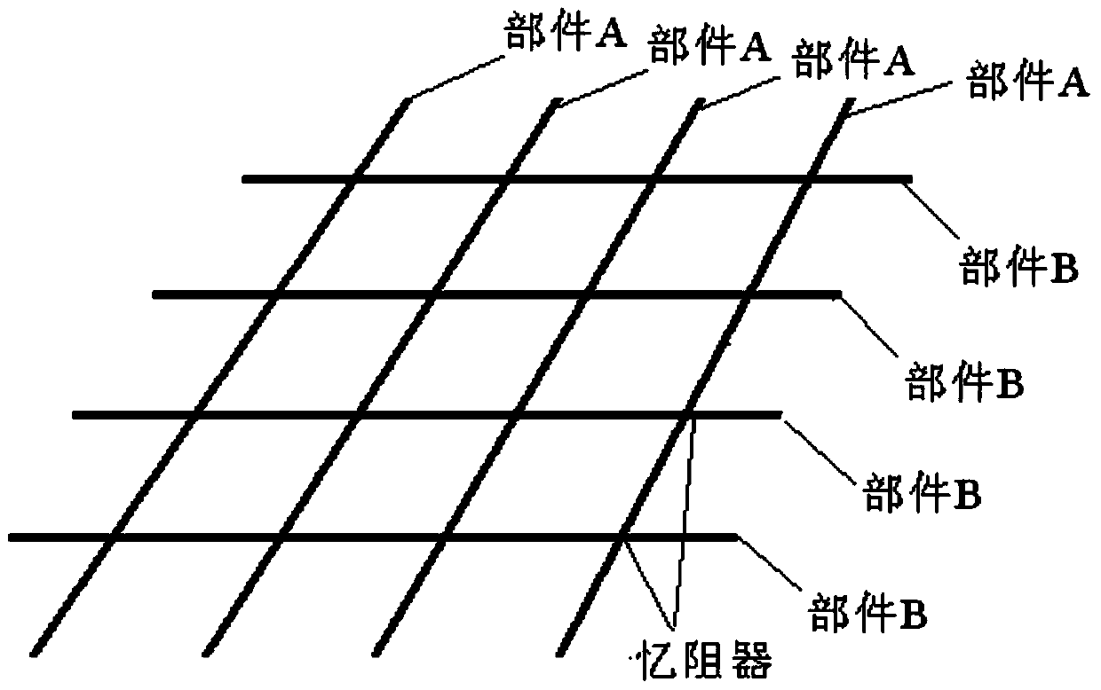
[0049] The preparation process process steps of the memristor of the present invention are as follows:

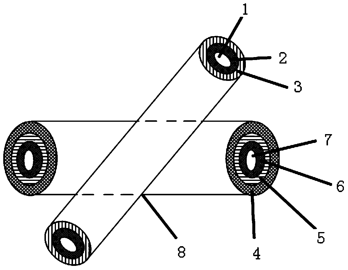
[0050] Step 1: using fiber 1 as flexible substrate I and fiber 7 as flexible substrate II;

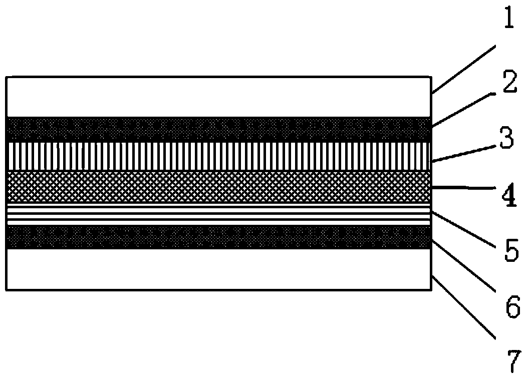
[0051] Step 2: Sputter a layer of Ta on the substrate I first, because Ta absorbs part of the natural oxide at the contact, reduces the contact resistance, and thus improves the adhesion to the electrode. Nitrogen gas is introduced while Ta is sputtered, and the process parameters are well controlled to form a TaN film with a thickness of about 100nm;

[0052] Step 3: adopt the same method as Step 2 to form a TaN film with a thickness of about 100 nm on the substrate II;

[0053] Step 4: On the TaN film (isolation layer 1) of the substrate 1, any one of epitaxy, chemical vapor deposition, electron beam evaporation, pulsed laser deposition, atomic layer deposition or magnetron sputtering Deposit a layer of conductive thin film with a thickness of 50nm-800nm ​​on it, and form an upp...

Embodiment 1

[0059] Both fiber 1 and fiber 4 are carbon fibers; the upper electrode material is Pt with a thickness of 200nm; the lower electrode material is Ag film with a thickness of 400nm; the storage medium layer is NiO with a thickness of 200nm.

Embodiment 2

[0061] Both fiber 1 and fiber 4 are glass fibers; the upper electrode material is Cu with a thickness of 800nm; the lower electrode material is W with a thickness of 50nm; the storage medium layer is Dy 2 o 3 , with a thickness of 50nm;


PUM

PropertyMeasurementUnit
thicknessaaaaaaaaaa
thicknessaaaaaaaaaa
thicknessaaaaaaaaaa

Abstract

The invention discloses a memristor based on a fiber substrate and a preparation method of the memristor. The memristor sequentially comprises a flexible fiber substrate I, an isolation layer I, an upper electrode, a storage dielectric layer thin film, a lower electrode, an isolation layer II and a flexible fiber substrate II from top to bottom. The preparation method of the memristor comprises the following steps of sequentially depositing the isolation layer I and the upper electrode on the surface of the flexible fiber substrate I to denote as a part A; sequentially depositing the isolation layer II, the lower electrode and the storage dielectric layer thin film on the surface of the flexible fiber substrate II to denote as a part B; and allowing the part A and the part B to contact at an arbitrary angle, and forming the memristor at a contact position. The memristor has the characteristics of favorable flexibility and light weight, can be bent, and is beneficial for promoting light-weight development of an electronic product; and the preparation method is compatible with the traditional complementary metal oxide semiconductor transistor (CMOS) process, is simple, is low in cost and high in production efficiency and has industrial value, and the demand for production at a large scale is met.

Description

technical field [0001] The invention relates to a memristor based on a fiber substrate and a preparation method thereof, belonging to the field of microelectronic devices. Background technique [0002] Memristor, also known as memristor, is a compound abbreviation of memory and resistance. The concept of memristor was first studied by Leon O.Chua, a scientist at the University of California, Berkeley. After the relationship between voltage and magnetic flux, it was proposed in 1971, and it was theoretically pointed out that memristor is the fourth basic passive circuit element after resistance, capacitance and inductance. It represents the relationship between charge and magnetic flux. Relationship. [0003] During the more than 30 years since the memristor was proposed, although the theory of memristor has developed, it has not attracted enough attention. Until 2008, Williams, a researcher at Hewlett-Packard Labs, successfully produced memristive elements based on metals ...

Claims


Application Information

Patent Timeline
Patent Type & Authority Patents(China)
IPC IPC(8): H01L45/00
Inventor 黄小忠谭飞龙蒋礼成雨果肖路军邹杨君韦永山
Owner CENT SOUTH UNIV
Why Eureka
Try Eureka