Organic semiconducting blend

A technology of semiconductors and blends, applied in the field of organic semiconductor blends

Inactive Publication Date: 2015-12-23
CAMBRIDGE DISPLAY TECH LTD
View PDF8 Cites 2 Cited by
  • Summary
  • Abstract
  • Description
  • Claims
  • Application Information

AI Technical Summary

Problems solved by technology

[0010] A second problem generally associated with blends of small molecule semiconductors and polymer semiconductors is that when the blends are deposited on surfaces with different surface regions, the crystallization of the small molecule semiconductors is often concentrated in some of these regions. In these, other regions are left where little or no small molecule semiconductor is present, resulting in films with regions of high and low concentrations of small molecule organic semiconductor

Method used


Image

  • Organic semiconducting blend
  • Organic semiconducting blend
  • Organic semiconducting blend

Examples


Embodiment

[0234] Material

[0235] Toluene and tetralin from Sigma-Aldrich

[0236] Fabrication Example of Organic Thin Film Transistor

[0237] (i) Pre-cleaning of OTFT substrate and self-assembled monolayer (SAM) pre-treatment:

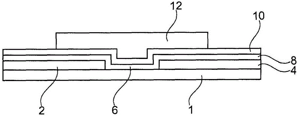
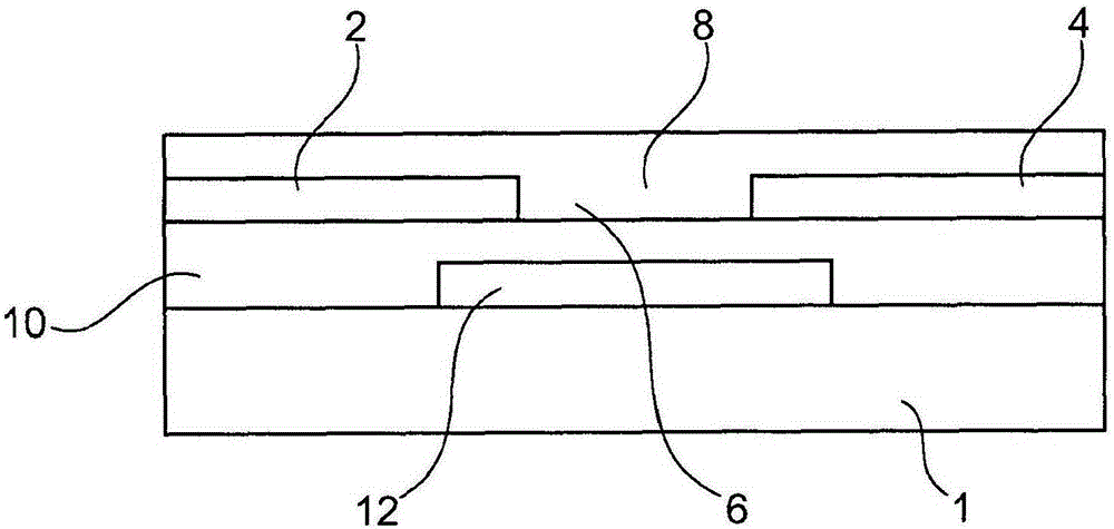
[0238] The first steps in device fabrication require pre-cleaning of the device substrate and application of surface treatment materials on the source and drain electrodes in order to ensure that contact resistance is minimized. The substrate consisted of gold source and drain electrodes (5 / 40 nmCr / Au) on top of a chromium adhesion layer on the glass surface. The substrate was cleaned by oxygen plasma to ensure removal of any remaining photoresist material (for source-drain definition).

[0239]After the plasma treatment, the electrode surface modifying compound (C 60 f 36 ). The solution was removed by spinning the substrate on a spin coater, which was then rinsed in toluene to remove any unreacted material that did not adsorb to the source and drain e...


PUM


Abstract

A blend for preparing a semiconducting layer an organic electronic device comprises a polymer, a first non-polymeric semiconductor, a second non-polymeric semiconductor and a third non-polymeric semiconductor. The blend enables higher concentration solutions of semiconductor and a broader solution processing window as compared to blends comprising one polymer and one non-polymeric semiconductor. For example, a blend comprising F8- TFB and three different substituted benzothiophene derivatives shows three-fold higher average saturation mobility in OTFTs as compared to a blend of one polymer and one of these benzothiophene derivatives and consistent peak saturation mobilities after drying at 60DEG, 80DEG and 100DEG even after a 2 minute delay.

Description

field of invention [0001] The present invention relates to blends and solutions for the preparation of semiconducting layers of organic electronic devices and to a method of preparing semiconducting layers of organic electronic devices comprising depositing the solution. The invention also relates to organic electronic devices comprising such blends and methods of making such devices. Background technique [0002] Transistors can be formed by processes in which the semiconductor layers of the transistor, and in many cases other layers, are deposited from solution. The resulting transistors are called thin film transistors. When an organic semiconductor is used in the semiconductor layer, the device is often described as an organic thin film transistor (OTFT). [0003] Various configurations of OTFTs are known. A device, a top-gate thin film transistor, includes a source and a drain, and a semiconductor layer is disposed between them in a channel region, a gate disposed ab...

Claims


Application Information

Patent Timeline
Patent Type & Authority Applications(China)
IPC IPC(8): H01L51/00H01L51/05
CPCH10K71/12H10K85/115H10K85/151H10K85/6576H10K10/466H10K10/464H10K10/462
Inventor C·纽萨姆
Owner CAMBRIDGE DISPLAY TECH LTD
Why Eureka
Try Eureka