Lead-free solder alloy

A technology of lead-free solder alloy and solder alloy, applied in the direction of welding/cutting medium/material, welding medium, welding equipment, etc., which can solve the adverse effects of increasing temperature performance and assembly quality, increasing energy consumption of electronic assembly, comprehensive energy To improve the resistance to mechanical shock and drop, improve the coarseness of Bi phase grains, and reduce the effect of poor welding

Inactive Publication Date: 2016-01-06
EUNOW ELECTRONICS TECH CO LTD SUZHOU
View PDF7 Cites 32 Cited by
  • Summary
  • Abstract
  • Description
  • Claims
  • Application Information

AI Technical Summary

Problems solved by technology

Although the above lead-free alloys avoid the use of Pb in traditional Sn/Pb solder alloys, which effectively protect the environment and human health, they have the following problems: ①The melting point of this type of lead-free alloy is in the range of 217-227°C, which is higher than that of traditional solder alloys. The melting point of Sn63Pb37 is 35-45°C. Therefore, in electronic assembly, the wave furnace or reflow furnace needs to be set at a higher temperature, which increases the energy consumption of electronic assembly.
According to statistics, a

Method used


Image

  • Lead-free solder alloy
  • Lead-free solder alloy
  • Lead-free solder alloy

Examples


Embodiment Construction

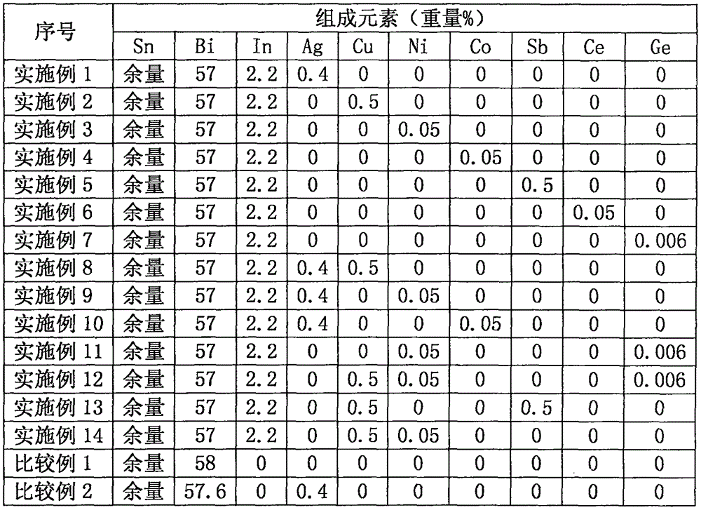
[0075] The specific examples of the present invention and the solder formulations of the comparative examples are shown in Table 1, wherein the contents of the main components Sn and Bi of the comparative examples 1 and 2 are basically the same as those of the examples so that performance comparisons can be carried out.

[0076] Table 1: Examples and Comparative Examples

[0077]

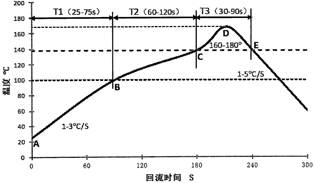
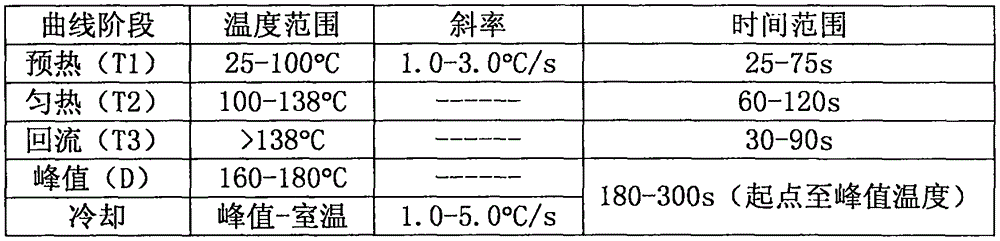
[0078] The steps of the manufacturing method of each of the above-mentioned embodiments are as follows:

[0079] (1) Melting Sn and In, microalloying elements Ag, Cu, Ni, Co, Mn, Ti, Sb and anti-oxidation elements P, Ge, Ga respectively in a vacuum induction heating furnace to form an intermediate alloy;

[0080] (2) smelting rare earth elements and Bi in a vacuum induction heating furnace to form rare earth alloys;

[0081] (3) Melt the rest of the Sn, Bi and Sn-In master alloys in a vacuum induction heating furnace at a melting temperature of 300-350°C, stir thoroughly for 60-90 minutes, then ...


PUM

PropertyMeasurementUnit
Melting pointaaaaaaaaaa

Abstract

The invention discloses a lead-free solder alloy. The lead-free solder alloy contains Bi of greater than or equal to 30% and less than or equal to 60%, In of greater than 2% and less than or equal to 5%, a microalloy element (a modificator), a rare-earth element, an anti-oxidization element, and the balance of Sn and inevitable impurities. The lead-free solder alloy is used for effectively improving the reliability problem of brittle fracture of a welded joint due to that Bi-phase crystalline grains in a traditional Sn-Bi alloy system are large and Bi is segregated at a Cu/Cu3Sn interface in the form of particles in the long-term service process of traditional Sn-Bi series alloys; as a result, the mechanical shock and the anti-dropping performance of the traditional Sn-Bi series alloys can be greatly improved.

Description

Technical field: [0001] The invention relates to the technical field of electronic welding, in particular to soldering by using a lead-free tin alloy, in particular to a low-melting-point Sn-Bi-In lead-free solder alloy. Background technique: [0002] Since electronic assembly became lead-free, Sn / Cu-based and Sn / Ag / Cu-based lead-free solder alloys are commonly used for wave soldering and reflow soldering processes. For example, in the wave soldering process, SnCu0.7, SnCu0.7-Ni, SnCu0.7-Si, SnAg0.3Cu0.7 (SAC0307) are commonly used, while in the reflow soldering process, SnAg3.0Cu0.5 (SAC305 ), SnAg3.8Cu0.7 (SAC387), SnAg1.0Cu0.5 (SAC105), SnAg0.3Cu0.7 (SAC0307), etc. Although the above lead-free alloys avoid the use of Pb in traditional Sn / Pb solder alloys, which effectively protect the environment and human health, they have the following problems: ①The melting point of this type of lead-free alloy is in the range of 217-227°C, which is higher than that of traditional sol...

Claims


Application Information

Patent Timeline
IPC IPC(8): B23K35/26
CPCB23K35/262B23K35/264
Inventor 罗登俊桑俊峰
Owner EUNOW ELECTRONICS TECH CO LTD SUZHOU
Why Eureka
Try Eureka