Method of forming fin field effect transistor, method of forming mos transistor

A fin field effect and transistor technology, which is applied to the formation of fin field effect transistors and the formation of MOS transistors, can solve problems such as metal residues, and achieve the effect of increasing density or hardness

Active Publication Date: 2018-03-30
SEMICON MFG INT (SHANGHAI) CORP
View PDF3 Cites 2 Cited by
  • Summary
  • Abstract
  • Description
  • Claims
  • Application Information

AI Technical Summary

Problems solved by technology

[0006] In the prior art, when the dielectric layer is planarized, recessed defects are easily generated in the dielectric layer, and metal residues are likely to be caused when the metal gate electrode is subsequently formed.

Method used


Image

  • Method of forming fin field effect transistor, method of forming mos transistor
  • Method of forming fin field effect transistor, method of forming mos transistor
  • Method of forming fin field effect transistor, method of forming mos transistor

Examples


Embodiment Construction

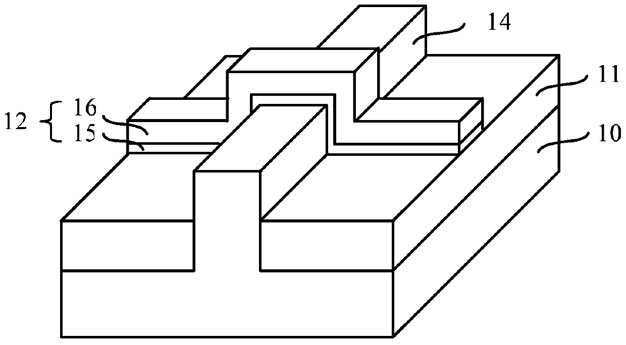
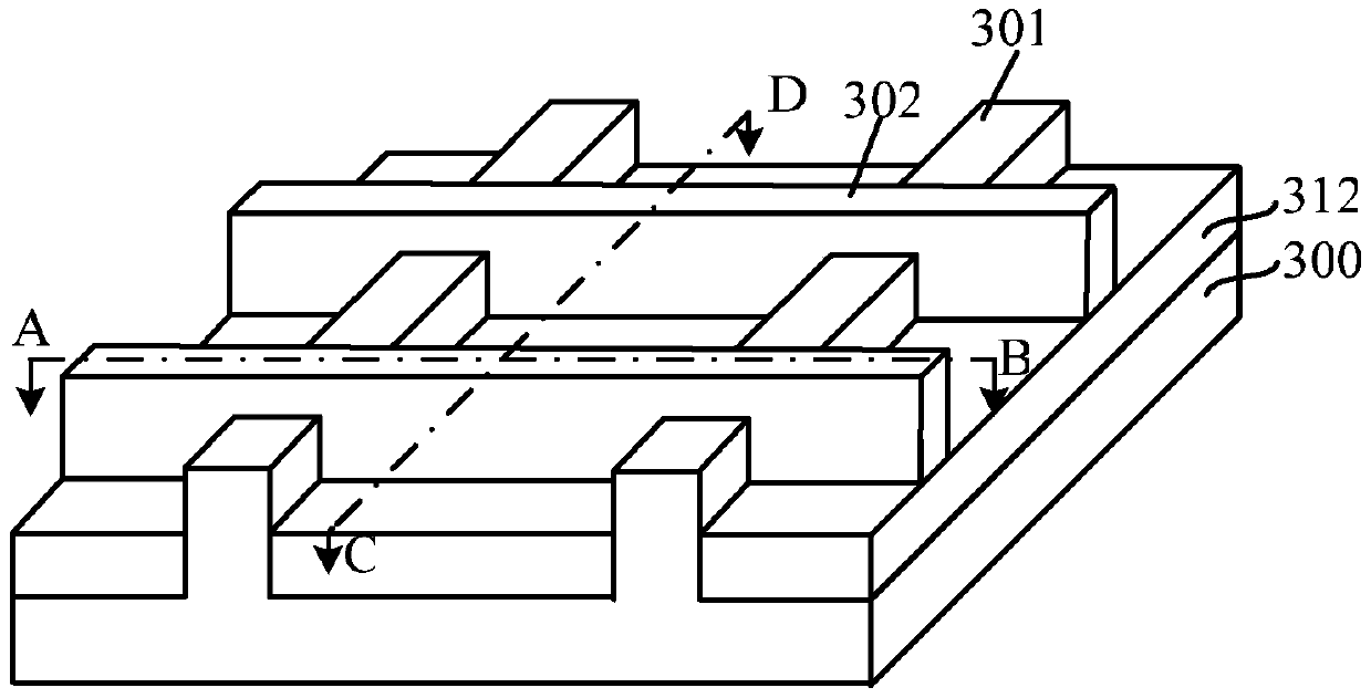
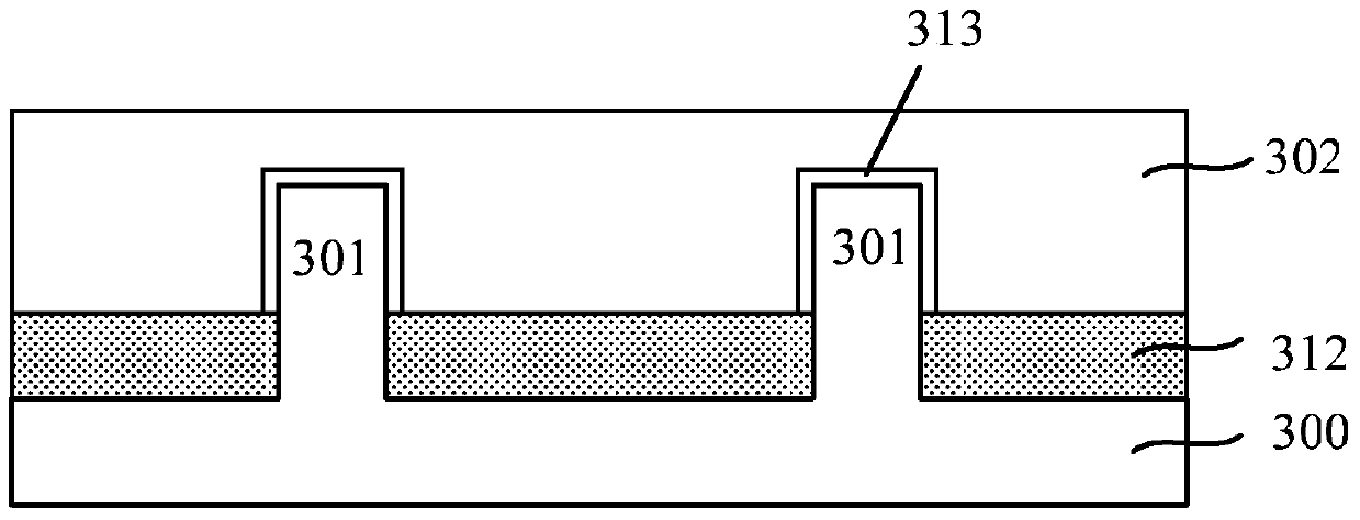
[0034]Since the fin field effect transistor has a special structure such as a fin and a gate structure across the sidewall and surface of the fin, when forming the dielectric layer, the gap between the fin and the gate structure and the gate structure It is difficult to fill the gaps well. In order to improve the gap filling performance of the dielectric layer, the prior art usually adopts the fluid chemical vapor deposition process to form the dielectric layer, although the dielectric layer formed by the fluid chemical vapor deposition has a higher gap filling performance. performance, but the material of the dielectric layer formed by fluid chemical vapor deposition is relatively soft or loose. The difference is very large, and it is very easy to form a dishing defect on the surface of the planarized dielectric layer. After removing the dummy gate to form a groove, when the metal gate is formed in the groove by deposition and chemical mechanical polishing process, some The m...


PUM


Abstract

A method for forming a fin field effect transistor and a method for forming a MOS transistor. The method for forming a fin field effect transistor includes: providing a semiconductor substrate on which several discrete fins are formed; forming a dummy gate across the sidewall and top surface of the fin; forming a dielectric layer covering the dummy gate and the semiconductor substrate, the surface of the dielectric layer being higher than the top surface of the dummy gate; performing a first ion implantation, Implanting solidified ions into the dielectric layer to increase the density of the dielectric layer; planarizing the dielectric layer to expose the surface of the dummy grid; removing the dummy grid to form a groove; forming a metal grid in the groove. The method of the present invention prevents pitting defects from being generated in the dielectric layer.

Description

technical field [0001] The invention relates to the field of semiconductor manufacturing, in particular to a method for forming a fin field effect transistor and a method for forming a MOS transistor. Background technique [0002] With the continuous development of semiconductor process technology, the process node is gradually reduced, and the gate-last (gate-last) process has been widely used to obtain an ideal threshold voltage and improve device performance. However, when the feature size (CD, Critical Dimension) of the device is further reduced, even if the gate-last process is adopted, the structure of the conventional MOS field effect transistor can no longer meet the requirements for device performance, and the fin field effect transistor (Fin FET) as a conventional Device substitution has received extensive attention. [0003] figure 1 A schematic structural view of a fin field effect transistor in the prior art is shown. Such as figure 1 As shown, it includes: ...

Claims


Application Information

Patent Timeline
Patent Type & Authority Patents(China)
IPC IPC(8): H01L21/336
Inventor 赵杰
Owner SEMICON MFG INT (SHANGHAI) CORP
Why Eureka
Try Eureka