Atomic layer deposition device and method

A technology of atomic layer deposition and equipment, applied in the direction of coating, metal material coating process, gaseous chemical plating, etc., can solve the problem that the back cleaning process time cannot be controlled, the cleaning effect cannot be achieved, and the silicon dioxide film cannot be removed cleanly, etc. problem, to achieve the effect of easy implementation, low cost and simple method

Active Publication Date: 2016-01-13
SHANGHAI INTEGRATED CIRCUIT RES & DEV CENT
View PDF4 Cites 4 Cited by
  • Summary
  • Abstract
  • Description
  • Claims
  • Application Information

AI Technical Summary

Problems solved by technology

However, since the thickness of the silicon dioxide film grown on the back of the silicon wafer cannot be controlled, the process time of the back cleaning cannot be controlled. If the back cleaning process time is too long, the dielectric film on the surface of the silicon wafer will also be cleaned; short, and cannot remove the excess silicon dioxide film on the back of the silicon wafer, and cannot achieve the ideal cleaning effect

Method used


Image

  • Atomic layer deposition device and method
  • Atomic layer deposition device and method

Examples


Embodiment Construction

[0027] In order to make the purpose, technical solution and advantages of the present invention clearer, the following will further describe the implementation of the present invention in detail in conjunction with the accompanying drawings. Those skilled in the art can easily understand other advantages and effects of the present invention from the contents disclosed in this specification. The present invention can also be implemented or applied through other different specific implementation modes, and various modifications or changes can be made to the details in this specification based on different viewpoints and applications without departing from the spirit of the present invention.

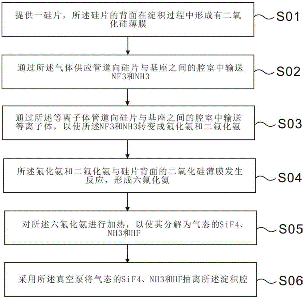
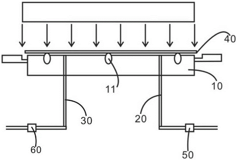
[0028] The above and other technical features and beneficial effects will be described in detail for the atomic layer deposition equipment and method of the present invention with reference to the embodiments and the accompanying drawings. figure 1 It is a schematic flow diagram of the ato...


PUM

PropertyMeasurementUnit
thicknessaaaaaaaaaa

Abstract

The invention belongs to the technical field of manufacturing technologies of semiconductor integrated circuits and discloses an atomic layer deposition device. The atomic layer deposition device comprises a substrate, a heating base, a gas supply pipe, a plasma pipe and a vacuum pump. Meanwhile, the invention discloses an atomic layer deposition method. The atomic layer deposition method includes the steps that firstly, NF3 and NH3 are conveyed into a cavity between a silicon wafer and the substrate; then plasma is introduced into the cavity to convert the NF3 and the NH3 into fluorinated ammonia and ammonia difluoride; the fluoride and a silicon dioxide film react to form ammonia hexafluoride; and then the ammonia hexafluoride is heated to be decomposed into gas and finally dissociated from a deposition cavity. By means of the atomic layer deposition device and method, the problems that an existing back cleaning technology is long in cleaning time and not thorough in cleaning are solved. The method is easy and convenient to implement, can be compatible with the existing technology, and has the beneficial effects of being low in cost, easy to implement and the like.

Description

technical field [0001] The invention belongs to the technical field of semiconductor integrated circuit manufacturing technology, and relates to an atomic layer deposition equipment and method. Background technique [0002] In the semiconductor integrated circuit industry, as the integration of semiconductor devices continues to increase and the critical dimensions associated with these devices continue to decrease, many new materials and processes are used in the device manufacturing process. For example, in the filling process of shallow trench isolation (STI), the traditional HDP technology can no longer be used, and large voids are prone to appear in the filling process, which affects the performance of the device. In the current filling process technology, atomic layer deposition equipment (Atomic Layer Deposition; ALD) is generally used to deposit a thin layer of silicon dioxide first, and then the HARP process is used for subsequent filling, so as to prevent the filli...

Claims


Application Information

Patent Timeline
Patent Type & Authority Applications(China)
IPC IPC(8): C23C16/455H01L21/205
Inventor 曾绍海李铭
Owner SHANGHAI INTEGRATED CIRCUIT RES & DEV CENT
Why Eureka
Try Eureka