Low-temperature polycrystalline silicon thin film transistor, manufacturing method, array substrate, and display panel

A technology of thin-film transistors and low-temperature polysilicon, which is applied in the direction of transistors, semiconductor/solid-state device manufacturing, semiconductor devices, etc., can solve problems such as interface defect state density, interface roughness, etc., to improve characteristics, simplify manufacturing process, and reduce interface roughness and the effect of interface defect state density

Active Publication Date: 2016-01-20
BOE TECH GRP CO LTD
View PDF4 Cites 9 Cited by
  • Summary
  • Abstract
  • Description
  • Claims
  • Application Information

AI Technical Summary

Problems solved by technology

Specifically, the low-temperature polysilicon thin film transistor and its manufacturing method, array substrate, and display panel of the present disclosure solve the problem of polysilicon active layer and g

Method used


Image

  • Low-temperature polycrystalline silicon thin film transistor, manufacturing method, array substrate, and display panel
  • Low-temperature polycrystalline silicon thin film transistor, manufacturing method, array substrate, and display panel
  • Low-temperature polycrystalline silicon thin film transistor, manufacturing method, array substrate, and display panel

Examples


Embodiment Construction

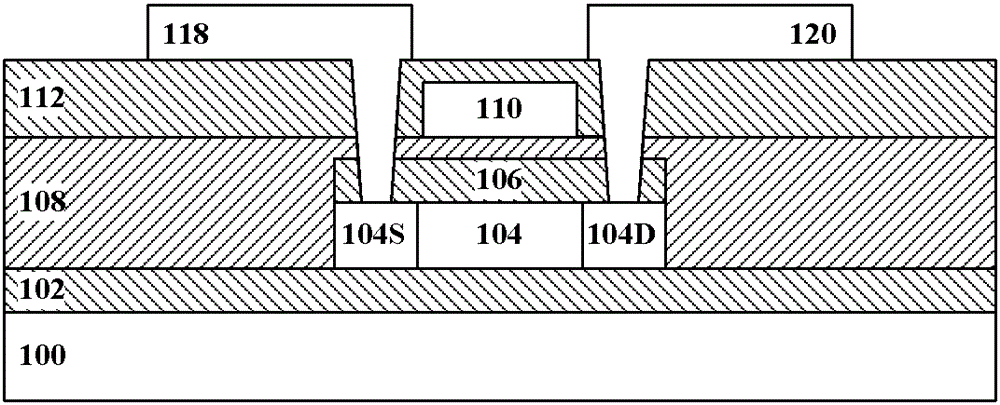
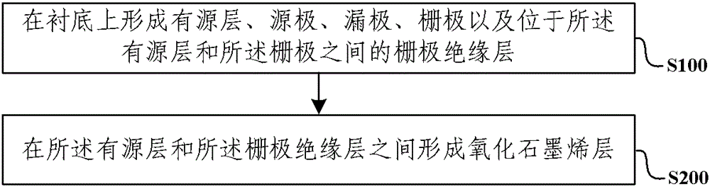
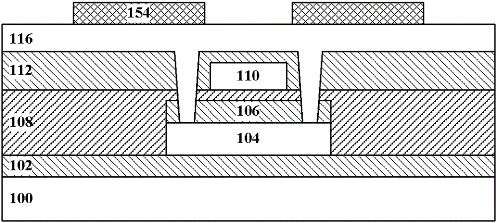
[0044] The specific implementation modes of the low-temperature polysilicon thin film transistor and its manufacturing method, array substrate, and display panel of the present disclosure will be described in detail below with reference to the accompanying drawings. The drawings of the present disclosure schematically show structures, parts and / or steps related to the invention, but not or only partially show structures, parts and / or steps not related to the invention. The thickness and shape of each film layer in the drawings do not reflect the true scale, but are only intended to schematically illustrate the content of the present disclosure.

[0045] The components shown in the drawings are labeled as follows:

[0046] 100, 200 substrates;

[0047] 102, 202 buffer layer;

[0048] 104, 210 active layer;

[0049] 104S source contact region;

[0050] 104D drain contact region;

[0051] 106, 208 graphene oxide layers;

[0052] 108, 206 gate insulation layer;

[0053] 110...


PUM

PropertyMeasurementUnit
Thicknessaaaaaaaaaa
Thicknessaaaaaaaaaa
Thicknessaaaaaaaaaa

Abstract

The invention relates to the technical field of display, and discloses a low-temperature polycrystalline silicon thin film transistor, a manufacturing method, an array substrate, and a display panel. The transistor comprises an active layer, a source electrode, a drain electrode, a grid electrode, a grid insulating layer disposed between the active layer and the grid electrode, and an oxidized graphene layer disposed between the active layer and the grid insulating layer, wherein the active layer, the source electrode, the drain electrode and the grid electrode are disposed on a substrate. The oxidized graphene layer is disposed between the active layer and the grid insulating layer, thereby reducing the interface roughness and the interface defect mode density between the active layer and the grid insulating layer. Moreover, there is no need to carry out pre-cleaning of the grid insulating layer. The invention also discloses the manufacturing method for the transistor, the array substrate, and the display panel.

Description

technical field [0001] The present disclosure relates to the field of display technology, and in particular to a low temperature polysilicon (LTPS) thin film transistor (thinfilm transistor, TFT) and a manufacturing method, an array substrate, and a display panel. Background technique [0002] LTP STFT liquid crystal display (liquid crystal display, LCD) is different from the traditional amorphous silicon (a-Si) TFT-LCD. The electron mobility of traditional amorphous silicon materials is only 0.5cm 2 / V.sec, while the electron mobility of low-temperature polysilicon can reach 50~200cm 2 / V.sec. Therefore, compared with the traditional amorphous silicon TFT-LCD, the low-temperature polysilicon TFT-LCD has advantages such as higher resolution, faster response speed, larger aperture ratio, and higher brightness. In addition, the high electron mobility allows the peripheral driver circuits to be integrated on the glass substrate to realize a system on glass (SOG), thereby sav...

Claims


Application Information

Patent Timeline
IPC IPC(8): H01L29/786H01L27/12H01L21/336
CPCH01L27/1222H01L29/66757H01L29/78675H01L29/78687H01L29/4908H01L29/66765H01L29/78696H01L29/78678H01L21/02112H01L21/02282H01L21/02318H01L27/1218H01L27/1248H01L27/1262H01L29/42384H01L29/513H01L29/6675H01L29/78603
Inventor 张帅詹裕程
Owner BOE TECH GRP CO LTD
Why Eureka
Try Eureka