Column-level ADC for high-speed linear CMOS image sensor and implement method

A technology of image sensor and implementation method, applied in the electrical field, capable of solving the problems of limiting the readout rate of CMOS image sensors, column-level fixed pattern noise, etc.

Inactive Publication Date: 2016-01-20
TIANJIN UNIV
View PDF3 Cites 14 Cited by
  • Summary
  • Abstract
  • Description
  • Claims
  • Application Information

AI Technical Summary

Problems solved by technology

[0005] (2) Mismatch between columns in the column-level A / D converter will introduce column-level fixed pattern noise
It can be seen that with the improvement of conversion accuracy, the conversion time increases exponentially, which greatly limits the readout rate of CMOS image sensors.

Method used


Image

  • Column-level ADC for high-speed linear CMOS image sensor and implement method
  • Column-level ADC for high-speed linear CMOS image sensor and implement method
  • Column-level ADC for high-speed linear CMOS image sensor and implement method

Examples


Embodiment Construction
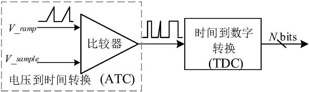
[0028] The basic idea of ​​the present invention is to use time to digital conversion (TDC) technology to divide the conversion process from analog to digital into two parts, figure 1 It is an overall architecture diagram of the present invention. The first part is the analog-to-time conversion (ATC), which consists of a ramp generator and a comparator that converts the input analog voltage into a proportional amount of time. The second part uses TDC to quantify the time interval width to complete the conversion from time to digital.

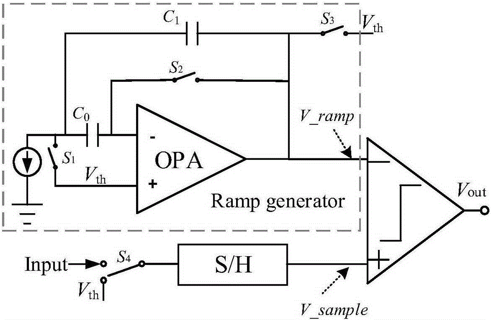
[0029] ATC consists of a ramp generator and a comparator, such as figure 2 As shown, it is used to generate a time signal proportional to the analog input voltage. As the front end of the entire ADC conversion, its linearity will directly affect the conversion accuracy of the entire ADC. In the present invention, in order to improve the linearity, the ramp generator adopts the integration of the current source and the cross-connected capacit...


PUM


Abstract

The invention relates to the analog to digital conversion technology, and aims to reduce the conversion time of a column-level single-slope ADC for a high scanning speed linear CIS without a significant increase in the area and power consumption. To this end, the invention adopts a technical scheme of a column-level ADC for a high-speed linear CMOS image sensor, and the column-level ADC is formed by series connection of an analog voltage to time converter (ATC) and a time to digital converter. The analog voltage to time converter ATC is constructed as follows: an input signal is connected to a same-phase end through a switch S4 and an S/H; and a current source positive end is connected through a capacitor to an OPA amplifier anti-phase end and is further connected through a switch S1 to bias voltage and an OPA amplifier same-phase end, a current source negative end is grounded, an OPA amplifier output end is connected with an anti-phase end, a switch S2 is disposed between the OPA amplifier output end and the anti-phase end, and a C1 is disposed between the OPA amplifier output end and the current source positive end. The invention is mainly applied to analog to digital conversion.

Description

technical field [0001] The invention belongs to the field of electricity and relates to an analog-to-digital conversion method, in particular to a column-level ADC of a high-speed linear array CMOS image sensor and a realization method thereof. Background technique [0002] A line image sensor obtains continuous images by scanning the target object in one or all directions. Therefore, they are commonly used in industrial inspection, aerial photography and satellite imaging. More and more applications require high-speed scanning to improve detection efficiency, and in some cases, the target object may be moving quickly. Both cases raise the need for high frame rate line scan image sensors. Among them, high-speed ADC is the key to high frame rate line array image sensor. [0003] Array-level ADCs achieve a good trade-off in power consumption, frame rate, silicon area, and fill factor. Therefore, array-level ADCs are widely used in line-array CMOS image sensors (CIS). But ...

Claims


Application Information

Patent Timeline
Patent Type & Authority Applications(China)
IPC IPC(8): H03M1/12
Inventor 姚素英杨聪杰徐江涛高静史再峰聂凯明高志远
Owner TIANJIN UNIV
Why Eureka
Try Eureka