Heterojunction high electron mobility spinning field effect transistor and manufacturing method

A high electron mobility, field effect transistor technology, used in semiconductor/solid state device manufacturing, circuits, electrical components, etc. The effect of optimizing the spin polarizability

Active Publication Date: 2016-02-03
SEMICON MFG ELECTRONICS (SHAOXING) CORP
View PDF4 Cites 3 Cited by
  • Summary
  • Abstract
  • Description
  • Claims
  • Application Information

AI Technical Summary

Problems solved by technology

[0004] However, the general spin field effect transistor injects spin electrons into semiconductors by ferromagnetic materials, but the efficiency of spin injection is only a few percent due to the mismatch of energy band structures of ferromagnetic materials such as Fe and semiconductor materials such as Sm.

Method used


Image

  • Heterojunction high electron mobility spinning field effect transistor and manufacturing method
  • Heterojunction high electron mobility spinning field effect transistor and manufacturing method

Examples


Embodiment Construction

[0029] The technical solutions of the present invention will be described in further detail below with reference to the accompanying drawings and embodiments.

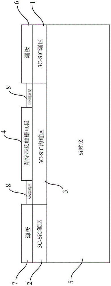
[0030] figure 1 It is a schematic diagram of the heterojunction high electron mobility spin field effect transistor of the present invention, as shown in the figure, specifically including 3C-SiC drain region 1, 3C-SiC source region 2, 3C-SiC channel region 3, Schottky Contact the gate electrode 4 , the Si substrate 5 , the drain 6 , the source 7 and the SiN isolation layer 8 .

[0031] The 3C-SiC drain region 1, the 3C-SiC source region 2, and the 3C-SiC channel region 3 are located on the Si substrate 5; the source electrode 7 is located on the 3C-SiC source region 2, and the Schottky contact gate electrode 4 is located on the 3C-SiC On the SiC channel region 3, the drain 6 is located on the 3C-SiC drain region 1; the SiN isolation layer 8 is located between the source 7 and the Schottky contact gate electrode 4, an...


PUM


Abstract

The invention relates to a heterojunction high electron mobility spinning field effect transistor and a manufacturing method. The transistor comprises a 3C-SiC drain region, a 3C-SiC source region, a 3C-SiC channel region, a Schottky contact gate electrode, an Si substrate, a drain electrode, a source electrode, and an SiN isolation layer. The 3C-SiC drain region, the 3C-SiC source region and the 3C-SiC channel region are located on the Si substrate. The source electrode is located in the 3C-SiC source region, the Schottky contact gate electrode is located in the 3C-SiC channel region, and the drain electrode is located in the 3C-SiC drain region. The SiN isolation layer is located between the source electrode and the Schottky contact gate electrode and between the Schottky contact gate electrode and the drain electrode. The transistor can change the doping density and defect density of source-drain materials through adjusting the dosage and annealing time of ion injection, thereby optimizing the spinning polarizability of the drain region and the source region under room temperature.

Description

technical field [0001] The invention relates to a heterojunction high electron mobility spin field effect transistor and a manufacturing method thereof, in particular to a heterojunction transistor which utilizes defective 3C-SiC doped with nitrogen atoms to inject source and drain electrodes to receive spin-polarized electrons. Mass junction high electron mobility spin field effect transistor and manufacturing method. Background technique [0002] With the rapid update of modern electronic technology, the development of traditional electronic devices has severely restricted the development of microelectronics science in terms of scale integration and computing speed. The emerging spintronics aims to conveniently regulate the spin of electrons, opening up a new field of information storage and transmission by using spin of electrons, which has caused research in multiple scientific fields such as physics, materials science and electronic information science. common concerns...

Claims


Application Information

Patent Timeline
Patent Type & Authority Applications(China)
IPC IPC(8): H01L29/778H01L29/06H01L21/335H01L21/265H01L21/324
CPCH01L21/265H01L21/324H01L29/06H01L29/66431H01L29/778
Inventor 贾仁需彭博吕红亮张玉明
Owner SEMICON MFG ELECTRONICS (SHAOXING) CORP
Why Eureka
Try Eureka