Organic field-effect tube of composite channel

A composite channel and organic field technology, which is applied in the manufacture of electrical components, electrical solid devices, semiconductor/solid devices, etc., can solve the problems of less interface and insufficient number of carriers, and achieve high switching current ratio and high current carrying capacity The effect of submobility

Inactive Publication Date: 2016-02-10
CHINA JILIANG UNIV
View PDF4 Cites 0 Cited by
  • Summary
  • Abstract
  • Description
  • Claims
  • Application Information

AI Technical Summary

Problems solved by technology

At present, many OFET active layers are horizontally stacked with N-type active layer and P-type active layer. In this structure, the interface between N-type active layer and P-type active layer is too small, resulting in the number of carriers generated by exciton dissociation. not enough

Method used


Image

  • Organic field-effect tube of composite channel

Examples


Embodiment Construction

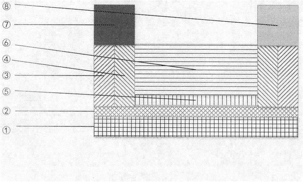
[0018] An organic field effect transistor with a composite channel, the preparation steps of which are as follows:

[0019] 1) The heavily doped silicon wafer was ultrasonically cleaned with acetone, ethanol, and deionized water for 30 minutes, and then dried in a glove box for 1 hour to clean the surface of the heavily doped silicon wafer;

[0020] 2) Place the above heavily doped silicon wafer in a UV / ozone environment for 120 minutes to obtain SiO 2 gate dielectric layer;

[0021] 3) On SiO 2 Positive photoresist is coated on the gate dielectric layer, and after pre-baking, exposure, development, and film hardening processes, ③ is obtained by photolithography. Pentacene active layer, control the evaporation rate as The vacuum degree is 1×10 -4 Pa; remove the glue after evaporation;

[0022] 4) Repeat step 3) to obtain ④ by photolithography, and the channel length is 200nm; then use the vacuum coating method to evaporate a 30nm thick C60 active layer on the heavily dop...


PUM


Abstract

The invention discloses an organic field-effect tube of a composite channel, and belongs to the field of microelectronic organic devices. The field effect characteristic of horizontal stacking organic field-effect tubes at the present stage is unsatisfactory, and cannot reach the requirement of modern integrated circuit technology. According to the organic field-effect tube of the composite channel provided by the invention, horizontal and longitudinal stacking composite active layers are formed by adopting photolithography and mask method, and the organic field-effect tube consists of a substrate, a gate electrode, a gate dielectric layer, the active layers, source and drain electrodes which are stacked in sequence. According to the structure, the interface amount of N-type active layers and P-type active layers is increased, the amount of current carriers generated through exciton dissociation is increased, and thus the field effect characteristic of the organic field-effect tube is improved. The organic field-effect tube of the composite channel can provide a novel idea for preparing the organic field-effect tube with good field effect characteristic, and has an important influence on commercialization application of the organic field-effect tube.

Description

【Technical field】 [0001] The invention belongs to the field of microelectronic organic devices, in particular to an organic field effect transistor with a composite channel. 【Background technique】 [0002] Organic Field Effect Transistor (OFET) has a series of advantages: it can be made into a large-area device, it is easy to adjust the performance of many materials, the preparation process is simple, the cost is low, and it has good flexibility. The research of OFET is to lay the foundation for the realization of all-organic circuits, so the research of high-performance OFET is more urgent. Modern integrated circuit technology requires good field effect transistor characteristics, such as high carrier mobility, large switching current ratio, and large subthreshold swing, but the current OFET is far from meeting the requirements of integrated circuit applications. The number of carriers is an important factor affecting the field effect characteristics of organic field effec...

Claims


Application Information

Patent Timeline
Patent Type & Authority Applications(China)
IPC IPC(8): H01L51/05H01L51/10
Inventor 陈真郑亚开唐莹韦一彭应全
Owner CHINA JILIANG UNIV
Why Eureka
Try Eureka