

Absorption layer for broadband spectrum pyroelectric detector and preparation method thereof
A pyroelectric detector and absorption layer technology, which is applied to electric radiation detectors and other directions, can solve the problems of difficulty in using line array and area array detectors, incompatibility with standard semiconductor processes, and weak adhesion of infrared absorption layers. Excellent heat transfer performance, firm adhesion and small specific heat capacity
- Summary
- Abstract
- Description
- Claims
- Application Information
AI Technical Summary
Problems solved by technology
Method used
Image

Examples
Embodiment 1
[0025] Based on LiTaO 3 In the unit pyroelectric detector of the material, the absorbing layer for the wide-spectrum pyroelectric detector of the present invention is adopted, and the preparation method of the absorbing layer for the wide-spectrum pyroelectric detector comprises the following steps:
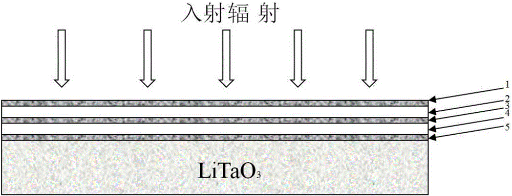
[0026] 1) Polished on both sides, the size is 1.2×1.2mm 2 LiTaO 3 Fabricate the absorbing layer on the wafer, and the two surfaces of the wafer are marked as A-side and B-side respectively. For LiTaO 3 Surface A of the wafer is mechanically thinned and planarized, and polished to a wafer thickness of 10 μm;
[0027] 2) Clean LiTaO 3 The wafer is photolithographically patterned on the A side to form an etching mask;
[0028] 3) In LiTaO 3 The third chromium-nickel alloy layer with a thickness of 7.5nm is deposited on the A side of the wafer by magnetron sputtering process;
[0029] 4) In LiTaO 3 The shape, structure and size of the electrode are etched on the A side of the ...
Embodiment 2
[0038] Based on LiTaO 3 The wide-spectrum pyroelectric detector absorbing layer of the present invention is adopted in the 32 × 1 pyroelectric array detector of the material, and the preparation method of the broad-spectrum pyroelectric detector using the absorbing layer comprises the following steps:
[0039] 1) Polished on both sides, the size is 1.2×1.2mm 2 LiTaO 3 Fabricate the absorbing layer on the wafer, and the two surfaces of the wafer are marked as A-side and B-side respectively. For LiTaO 3 Surface A of the wafer is mechanically thinned and planarized, and polished to a wafer thickness of 10 μm;
[0040] 2) Clean LiTaO 3 The wafer is photolithographically patterned on the A side to form an etching mask;
[0041] 3) In LiTaO 3 The third chromium-nickel alloy layer with a thickness of 8.5nm is deposited on the A side of the wafer by magnetron sputtering process;
[0042] 4) In LiTaO 3 The shape, structure and size of the electrode are etched on the A side of th...
PUM
| Property | Measurement | Unit |
|---|---|---|
| thickness | aaaaa | aaaaa |
| thickness | aaaaa | aaaaa |
| thickness | aaaaa | aaaaa |
Abstract
Description
Claims
Application Information