

Integration method of vertical nano-wire transistor
An integration method, nanowire technology, applied in nanotechnology, nanotechnology, nanotechnology for information processing, etc., can solve problems such as limiting the improvement of device performance and difficult to use gate-last process, to improve consistency, avoid Etch damage and performance improvement effect
- Summary
- Abstract
- Description
- Claims
- Application Information
AI Technical Summary
Problems solved by technology
Method used
Image

Examples
Embodiment 1
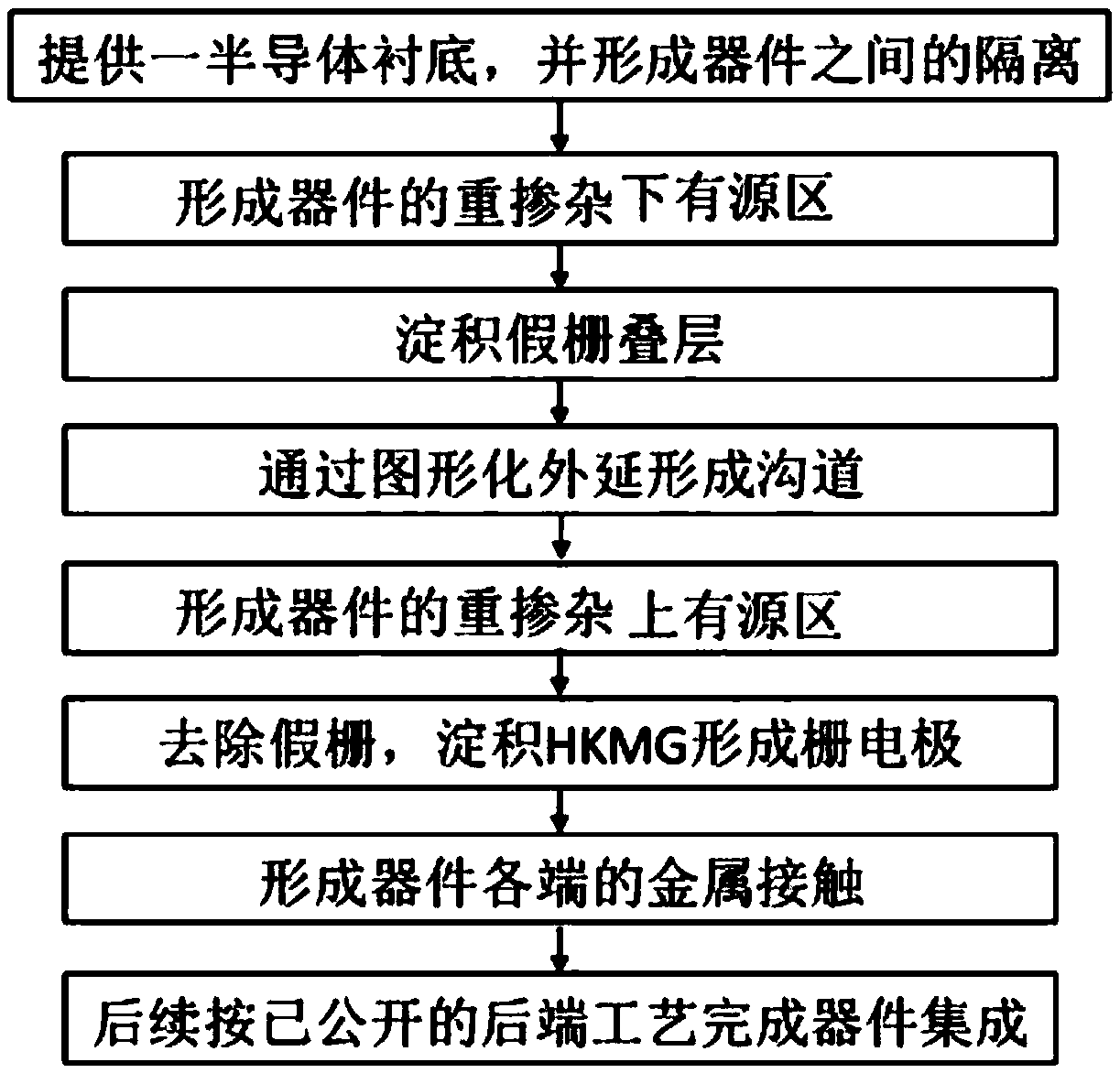
[0094] The CMOS integration of bulk silicon vertical nanowire devices with a diameter of 6nm can be realized according to the following steps (the structure parameters are set according to the High-Performance device of the "11 / 10nm" technology generation in ITRS-2013):
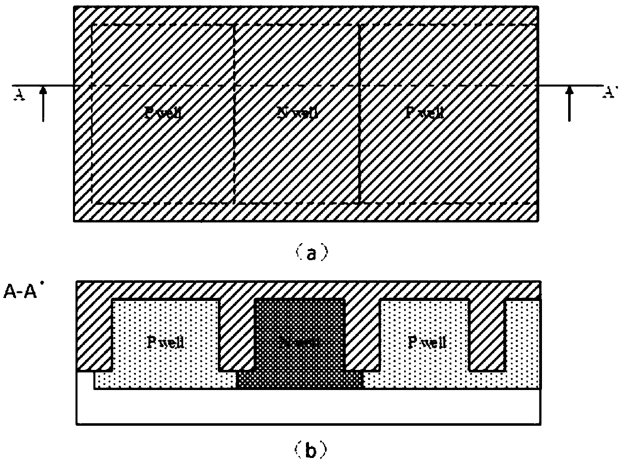
[0095] 1) Form a double well (Nwell / Pwell), SiO on a (100) bulk silicon substrate according to the published bulk silicon process 2 Shallow Trench Isolation (STI), the surface is planarized by Chemical-Mechanical Polishing (CMP), and the substrate surface retains 50nmSiO 2 ,Such as figure 2 Shown
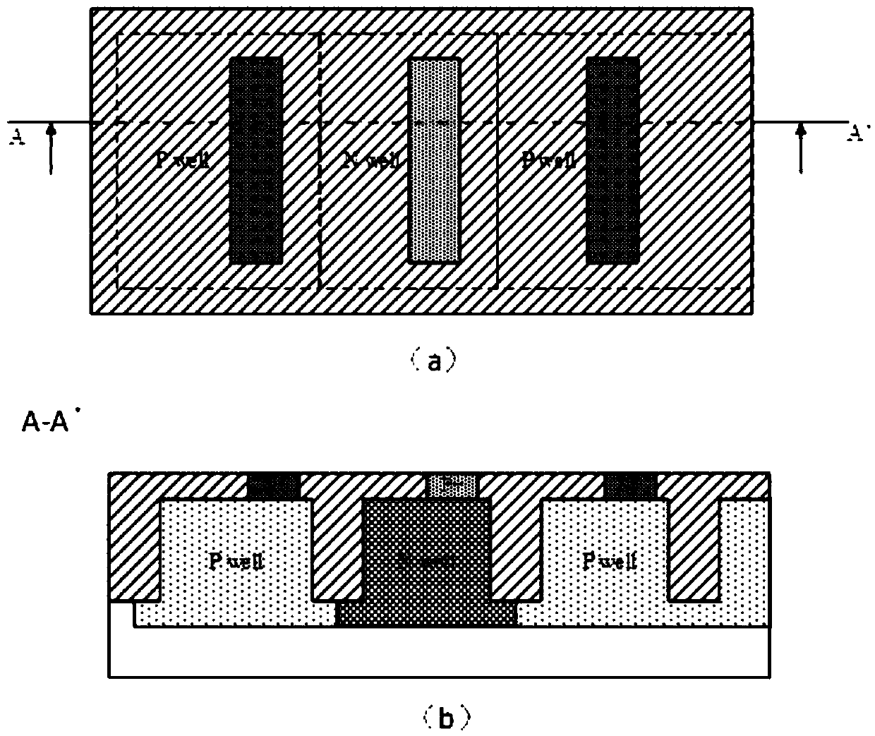
[0096] 2) Form the epitaxial window of the active area under the device by photolithography and anisotropic etching;
[0097] 3) P+ heavily doped active regions (as the source / drain terminals of PMOS) are formed on the Nwell by in-situ doped epitaxial processes, and N+ heavily doped active regions (as the source of NMOS) are formed on the Pwell. / Drain), such as image 3 Shown
[0098] 4) Deposit 5nmSiO sequentially by AL...
Embodiment 2
[0121] According to the following steps, the hybrid integration of vertical nanowire devices (such as Si-NMOS and Ge-PMOS) with a diameter of 4.5nm with two material channels on an SOI substrate can be realized (the structure parameters are based on ITRS-2013 "8 / 7nm" High-Performance device of technology generation to set):
[0122] 1) Epitaxy 20nm GeSi on a (100) SOI substrate, and do N+ and P+ respectively to form the lower active region of the device (as the source / drain of the device);
[0123] 2) The isolation of the active area under the N / P device is realized by photolithography and etching, such as Figure 19 Shown
[0124] 3) Through LPCVDSiO 2 STI is formed, and the surface is planarized by CMP to expose the upper surface of the heavily doped active region;
[0125] 4) Deposit 3nmSiO sequentially by ALD 2 (As the SDE mask layer 1, its thickness defines the length of the device's source and drain extension SDE is 3nm), 14nmSi3N4 (fake gate layer, its thickness defines the cha...
PUM
 Abstract
Description
Claims
Application Information