Embedded nanometer forest structure and preadaptation method thereof

An embedded, nanotechnology, applied in the field of nanometers, can solve problems such as difficult formation of microchannel structures

Active Publication Date: 2016-03-09
苏州研材微纳科技有限公司
View PDF8 Cites 9 Cited by
  • Summary
  • Abstract
  • Description
  • Claims
  • Application Information

AI Technical Summary

Problems solved by technology

[0005] The invention provides an embedded nano-forest structure and its preparation method to solve the problem that it is not easy to for

Method used


Image

  • Embedded nanometer forest structure and preadaptation method thereof
  • Embedded nanometer forest structure and preadaptation method thereof
  • Embedded nanometer forest structure and preadaptation method thereof

Examples


Embodiment 1

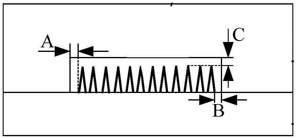
[0059] In this embodiment, the substrate 100 is a bulk silicon substrate, the etch stop layer 101 is a silicon dioxide film, and the opening exposes the substrate 100 to form the material of the nano mask structure 2011 Is a negative photoresist, and the nano structure shape of the nano forest structure 1001 is tapered. Figure 6G As shown, the method includes:

[0060] Step S01, a substrate 100 is provided, such as Figure 6A Shown.

[0061] In the embodiment of the present invention, the substrate 100 is used to form the embedded nano-forest structure 1001 and provide support for subsequent processes. The substrate 100 may be any suitable substrate in the micromachining process. In an embodiment, the substrate 100 is a single crystal silicon substrate.

[0062] Step S02, forming an etching stopper layer 101 with openings on the substrate 100, such as Figure 6B Shown.

[0063] In this embodiment, the etching stop layer 101 having an opening 1011 is formed on the substrate 100. The ...

Embodiment 2

[0083] The manufacturing method of the embedded nano-forest structure 1001 is as described in the first embodiment, the difference is that in this embodiment, the substrate 100 is a silicon-on-insulator (SOI) substrate; the etching barrier layer 101 is a silicon nitride film; the method further includes: before forming a nano mask structure 2011 on the surface of the substrate 100, depositing a hard mask layer 501 with a thickness of 50-100 nm on the surface of the substrate 100 After the nano mask structure 2011 is formed thereon, anisotropic etching is performed to form a nano hard mask structure 5011 in the hard mask layer 501, using the nano hard mask structure 5011 as a mask; the in-cell type The nano structure shape of the nano forest structure 1001 is columnar, mesa, and a combination of planes; the material of the nano mask structure 2011 is silicon dioxide, and uniformly distributed nanometers are formed on the substrate 100 by a spin coating method. The particle array...

Embodiment 3

[0094] In this embodiment, different from the first embodiment, the substrate 100 is a quartz substrate; the etching stop layer is a 100-300 nm silicon nitride film; the opening 1011 does not expose the substrate 100, Control the formation of the etching depth of the etching stop layer 101; the polymer layer 201 is a patterned polymer layer 201', and the patterned polymer layer 201' is a photosensitive polyimide layer or a nanoimprint film Layer; such as Figure 8A to Figure 8D Shown.

[0095] In step S21, the substrate 100 is provided.

[0096] In this embodiment, the substrate 100 is a quartz substrate, which has a lower cost than a silicon substrate and is more suitable for mass production applications.

[0097] In step S22, an etching stop layer 101 having an opening 1011 is formed on the substrate 100. The difference from the first embodiment is that the opening 1011 does not expose the substrate 100. Preferably, a photolithography process and When the opening 1011 is obtained...


PUM

PropertyMeasurementUnit
Thicknessaaaaaaaaaa
Thicknessaaaaaaaaaa
Thicknessaaaaaaaaaa

Abstract

The invention discloses an embedded nanometer forest structure and a preadaptation method thereof. The method comprises: providing a substrate; forming an etching stopping layer with an opening on the substrate; forming a nanometer masking structure on the surface of the substrate; performing anisotropic etching, and forming the embedded nanometer forest structure at the opening of the substrate; and removing the nanometer masking structure and the etching stopping layer. The top of the embedded nanometer forest structure can be in seamless joint with the smooth surface of another substrate, and the nanometer masking structure can totally covers the opening area, a gap can not be formed in the edge part of the embedded nanometer forest structure after the anisotropic etching, and DNA molecules can be prevented from flowing through the gap between the nanometer forest structure and a microchannel.

Description

Technical field [0001] The invention belongs to the field of nanotechnology, and in particular relates to an embedded nano forest structure and a preparation method thereof. Background technique [0002] Large-area nanostructures exhibit super affinity / hydrophobicity, enhanced surface plasmon oscillation, field emission, light filtering, etc. due to the structural characteristics of large surface-to-body ratio, large roughness, large surface area, tip, multiple pores / gaps, etc. Light absorption and other characteristics, so it is often suitable for self-cleaning surfaces, microfluidic devices, surface enhanced Raman scattering devices, surface plasma infrared absorption devices, biomedical detection devices such as DNA molecular separation devices or functional devices, optoelectronic devices, optical sensor devices , Solar cells and other new energy devices, and some other applications. In recent years, large-area nanostructures have become a research focus. The large-area na...

Claims


Application Information

Patent Timeline
IPC IPC(8): B81C1/00B81B1/00
CPCB81B1/00B81C1/00031
Inventor 毛海央
Owner 苏州研材微纳科技有限公司
Why Eureka
Try Eureka