

Self-reference interference alignment system
A self-reference interference and alignment system technology, applied in the field of semiconductor manufacturing, can solve the problems of unstable optical structure, uncompact optical structure, multi-optical noise, etc., to improve engineering achievability, expand size, and reduce manufacturing difficulty. Effect
- Summary
- Abstract
- Description
- Claims
- Application Information
AI Technical Summary
Problems solved by technology
Method used
Image

Examples
Embodiment 1
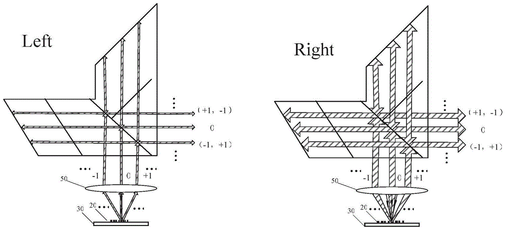
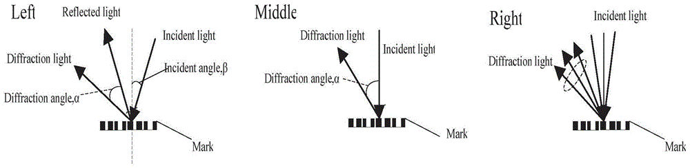
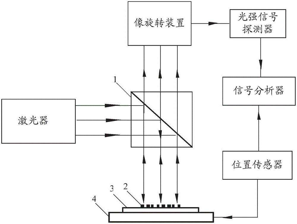
[0037] Please refer to figure 2 , in this embodiment, a self-referencing interference alignment system is proposed, including: a light source, a lens 50, a self-referencing interference alignment optical module, a signal detection module and an alignment mark 20, wherein the light source is used to provide illumination light beam, the illumination beam forms a cone-shaped beam or a projection beam of a conical beam after passing through the lens 50, and irradiates onto the alignment mark 20 to form a diffracted light class of positive and negative diffraction orders, and the diffracted spot is fed back to the self-reference In the interference optics module, the self-reference interference optics module performs image rotation processing on the diffraction spot so that the images of the corresponding positive and negative order diffraction spots overlap, and the signal detection module is used to detect the overlapped positive and negative order Diffraction spot image.
[00...
Embodiment 2
[0062] In this embodiment, the devices included in the proposed self-referencing interferometric alignment system are the same as those in Embodiment 1, the difference is that, as Figure 9 As shown, the alignment mark 20 includes the grating period P1 of the first alignment mark and the grating period P2 of the second alignment mark, and the grating period P1 of the first alignment mark and the grating period P2 of the second alignment mark are not etc. For example, the grating period P1 of the first alignment mark is a period of 8 microns, and the grating period P2 of the second alignment mark is a period of 8.8 microns. In this way, it is easier to distinguish alignment.
[0063] The specific alignment operation method and signal processing operation are the same as those in the first embodiment, and will not be repeated here. For details, please refer to the first embodiment.
Embodiment 3
[0065] In order to expand the scope of capture, more marked branches can be adopted, such as Figure 10 shown. Wherein, the alignment marks 20 include multiple groups, which are divided into a first group of alignment marks and a second group of alignment marks, the first group of alignment marks includes a plurality of first alignment marks, and the second group of alignment marks The marks include a plurality of second alignment marks, the first group of alignment marks and the second group of alignment marks are arranged at intervals along the scanning direction, and the predetermined inclination angle between the first alignment marks and the scanning direction is 45 degrees , the predetermined inclination angle between the second alignment mark and the scanning direction is 135 degrees, and the first group of alignment marks and the second group of alignment marks have the same grating period or different grating periods. Specifically, in this embodiment, the two marking...
PUM
 Abstract
Description
Claims
Application Information