High-power 808nm DFB LD built-in grating preparation method

A high-power, grating technology, applied in the field of holographic exposure and wet etching process, can solve the problems of distributed feedback lasers, such as difficulty in ensuring narrow linewidth, small wavelength drift, and difficult preparation processes, and achieves good wavelength drift, good The effect of surface morphology, narrow line width

Inactive Publication Date: 2016-03-16
CHANGCHUN UNIV OF SCI & TECH
View PDF0 Cites 5 Cited by
  • Summary
  • Abstract
  • Description
  • Claims
  • Application Information

AI Technical Summary

Problems solved by technology

The grating layer of the 808nm distributed feedback laser is developing towards Al-free materials such as InGaP, which solves the problem that Al-containing materials are easy to oxidize, but InGaP brings difficulties to the traditional preparation process
As far as the existing technology is concerned, it is difficult to guarantee a narrow linewidth and a small wavelength drift for the prepared distributed feedback laser.

Method used


Image

  • High-power 808nm DFB LD built-in grating preparation method
  • High-power 808nm DFB LD built-in grating preparation method

Examples


Embodiment Construction

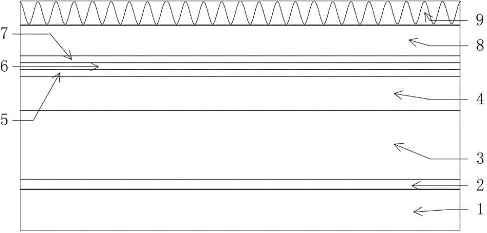
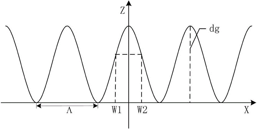
[0014] The purpose of the present invention is to provide a preparation process of a built-in grating in a high-power 808nm distributed feedback laser. In order to achieve the above object, the preparation process of the built-in grating of the high-power 808nm distributed feedback semiconductor laser provided by the present invention is completed by combining holographic exposure and wet etching. The main steps are:

[0015] A) An epitaxial growth is carried out by MOCVD. The first epitaxial growth step is: respectively grow 0.5mm N-GaAs (Si doped, 2.0′10 mm) on the GaAs substrate 18 cm -3 ) buffer layer, 0.05mm N-Ga x al 1-x As (x=0.05~0.55, Si-doped, ~1.0′10 18 cm -3 ) Gradient transition layer, 1.2mm N-Al 0.55 Ga 0.45 As (Si doped, 1.0′10 18 cm -3 ) lower confinement layer, 0.15mm of unintentionally doped Al x Ga 1-x As (x=0.55~0.25) graded waveguide layer, 5nm unintentionally doped Al 0.25 Ga 0.75 As quantum well barrier layer, 4nm unintentionally doped Al 0....


PUM


Abstract

The invention aims to prepare a distributed feedback Bragg grating suitable for a high-power 808nm semiconductor laser by using holographic lithography and wet etching process, and relates to the technical field of semiconductor device manufacture. The invention is characterized by comprising the steps of carrying out one-time epitaxial growth on a GaAs substrate by using metal organic chemical vapor deposition (MOCVD) technology; exposing the prepared epitaxial wafer by using a holographic exposure system with an exposure source being a 325nmHe-Cd laser; carrying out developing and hardening; and finally, etching an InGaP grating layer by using an etching solution with a volume ratio of HCl:C2H6O2=3:2 and obtaining a grating. The beneficial effects of the invention are that a second-order grating with better morphology is prepared on the InGaP grating layer and the duty cycle, groove depth and other parameters enables the laser to have narrow linewidth and small wavelength shift. Meanwhile, the process can be used for high-power compound semiconductor laser of other wavelength and has a wide range of application.

Description

technical field [0001] A method for preparing a built-in grating of a high-power 808nm DFB distributed feedback semiconductor laser, especially a method for preparing a second-order distributed feedback Bragg grating on the InGaP grating layer. The invention belongs to the technical field of semiconductor device manufacturing, including holographic exposure and wet etching processes. Background technique [0002] The technique of using built-in gratings to lock the wavelength of semiconductor lasers has been studied for nearly half a century. Distributed feedback laser is the product of this technology. With the progress of optical fiber communication in the 1980s and 1990s, it developed most rapidly in the 1.3μm and 1.55μm bands. Compared with distributed feedback semiconductor lasers in this band, the development of GaAs-based short-wave distributed feedback lasers seems to lag behind. The main reason for this phenomenon is that these short-wavelength lasers are not wide...

Claims


Application Information

Patent Timeline
Patent Type & Authority Applications(China)
IPC IPC(8): H01S5/12
Inventor 曲轶郭海侠石宝华高峰李再金李辉乔忠良张晶
Owner CHANGCHUN UNIV OF SCI & TECH
Why Eureka
Try Eureka