Folded external cavity ultra-narrow linewidth semiconductor laser

An ultra-narrow linewidth and laser technology, which is applied to the device for controlling the output parameters of the laser, the structure of the optical resonant cavity, etc., to achieve the effect of not easy mode hopping, narrow laser linewidth, and increased integration

Active Publication Date: 2018-06-05
CHANGCHUN INST OF OPTICS FINE MECHANICS & PHYSICS CHINESE ACAD OF SCI
View PDF3 Cites 1 Cited by
  • Summary
  • Abstract
  • Description
  • Claims
  • Application Information

AI Technical Summary

Problems solved by technology

[0005] In order to solve the problems existing in the prior art, the present invention provides a folded external cavity ultra-narrow linewidth semiconductor laser, which mainly solves the problem of realizing ultra-narrow linewidth semiconductor lasers on the chip scale

Method used


Image

  • Folded external cavity ultra-narrow linewidth semiconductor laser
  • Folded external cavity ultra-narrow linewidth semiconductor laser
  • Folded external cavity ultra-narrow linewidth semiconductor laser

Examples


Embodiment 1

[0027] Embodiment 1: A method for preparing a folded external cavity ultra-narrow linewidth semiconductor laser, comprising the following steps:

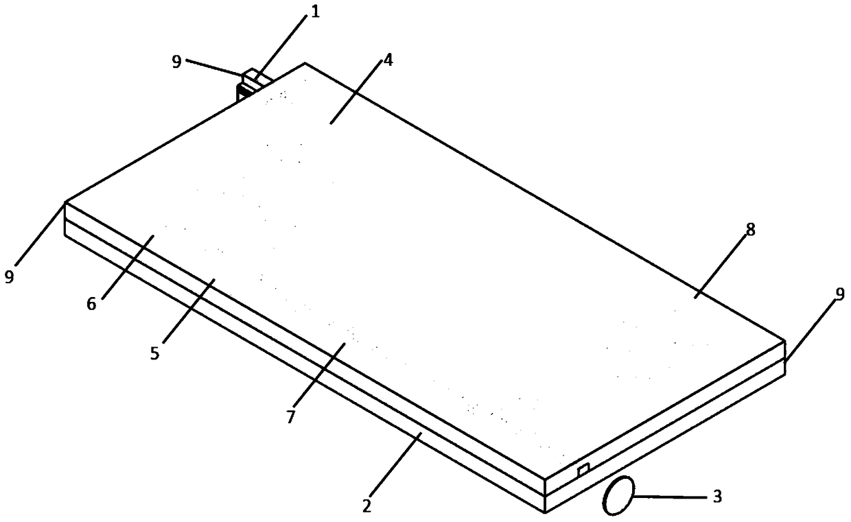
[0028] Step 1: Prepare an InP-based semiconductor laser chip 1 that emits light near a wavelength of 1550 nm.

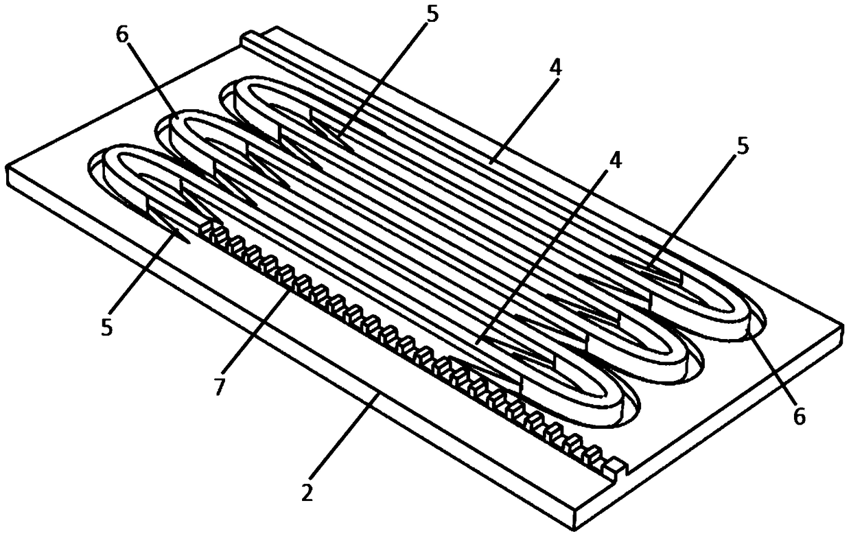
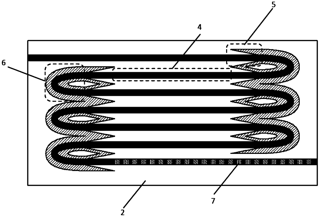
[0029] Step 2: Use SOI sheet as the folded external cavity 2 chip, SOI is a commercial silicon on insulator chip, its typical structure is the substrate Si, and the isolation layer is SiO 2 , the working layer is Si. The single-wavelength reflective structure 7 is prepared by photolithography. The single-wavelength reflective structure 7 is a first-order grating. The spectral reflection peak of its waveguide is located at 1550nm±1nm, and the reflection bandwidth is smaller than the longitudinal mode interval of the folded external cavity ultra-narrow linewidth semiconductor laser.

[0030] Step 3: Grow a layer of SiO with a thickness of 1 μm by PECVD 2 The single-wavelength reflective structure 7 is protected as a gratin...


PUM


Abstract

The folded external cavity ultra-narrow linewidth semiconductor laser belongs to the technical field of new semiconductor lasers. The laser includes: a semiconductor laser chip, a folded external cavity and a shaping lens; The end face of the cavity makes the cavity film; the shaping lens is located at the output end of the folded external cavity. The curved waveguide structure in the folded external cavity of the present invention effectively filters high-order modes, ensures almost loss-free transmission of the fundamental mode, has more stable mode characteristics, and is less prone to mode hopping. By folding the external cavity instead of the straight waveguide, it is more beneficial to obtain a narrow linewidth laser of the kHz order, and integrate a semiconductor laser external cavity structure with a length of several tens of times on a very short external cavity chip, which reduces the volume of the package and increases the cost. Integration level, simple and effective to get narrower laser linewidth. The overall packaging of the device is carried out in the form of a waveguide external cavity, which increases the stability of the system and makes the system suitable for various complex use environments.

Description

technical field [0001] The invention belongs to the technical field of novel semiconductor lasers, in particular to a folded external cavity ultra-narrow linewidth semiconductor laser. Background technique [0002] In the laser carrier communication system, a high-performance narrow-linewidth semiconductor laser (linewidth ≤ 10kHz) is the core component that determines the ranging accuracy, because for a narrow-linewidth laser with a 3kHz linewidth, its coherence length can reach 100km. In addition, narrow-linewidth semiconductor lasers have extremely wide applications in the fields of ultra-high-precision lidar, ship hydrophone, spacecraft docking, inter-satellite communication, coherent optical communication, laser spectroscopy, atmospheric absorption measurement and optical fiber communication. The military value, economic value and scientific value of the system served by the narrow linewidth laser are very large, it plays a key role in these systems, and its position is...

Claims


Application Information

Patent Timeline
Patent Type & Authority Patents(China)
IPC IPC(8): H01S5/14H01S5/06
Inventor 陈泳屹秦莉宁永强王立军
Owner CHANGCHUN INST OF OPTICS FINE MECHANICS & PHYSICS CHINESE ACAD OF SCI
Why Eureka
Try Eureka