

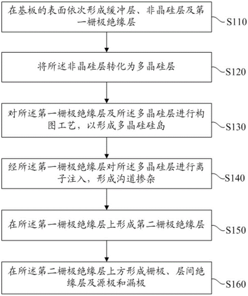
Thin-film transistor and preparation method thereof
A technology of thin film transistors and polysilicon, which is applied in the direction of transistors, semiconductor/solid-state device manufacturing, semiconductor devices, etc., and can solve problems such as long process time, channel effect, and large surface damage of polysilicon
- Summary
- Abstract
- Description
- Claims
- Application Information
AI Technical Summary
Problems solved by technology
Method used
Image

Examples
Embodiment Construction
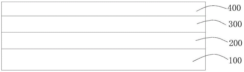
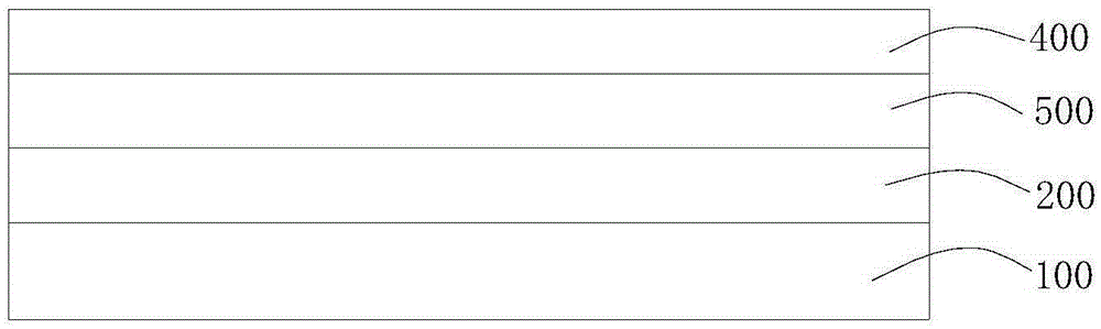
[0031] In order to make the above-mentioned objects, features and advantages of the present invention more obvious and understandable, the specific embodiments of the present invention will be described in detail below with reference to the accompanying drawings. In the following description, many specific details are explained in order to fully understand the present invention. However, the present invention can be implemented in many other ways different from those described herein, and those skilled in the art can make similar improvements without departing from the connotation of the present invention. Therefore, the present invention is not limited by the specific implementation disclosed below.
[0032] It should be noted that when an element is referred to as being "fixed to" another element, it can be directly on the other element or a central element may also exist. When an element is considered to be "connected" to another element, it can be directly connected to the ot...
PUM
| Property | Measurement | Unit |
|---|---|---|
| thickness | aaaaa | aaaaa |
| thickness | aaaaa | aaaaa |
| thickness | aaaaa | aaaaa |
Abstract
Description
Claims
Application Information