Intelligent wafer cutting machine

A technology for cutting machine tools and wafers, which is applied to work accessories, fine work devices, stone processing equipment, etc., can solve the problems of low production process efficiency, high electronic equipment prices, high costs, and improve cutting accuracy and automation. , Improve the success rate of cutting, optimize the effect of modules and designs

Inactive Publication Date: 2016-03-30
HENAN GUANGDU SUPERHARD MATERIAL CO LTD
View PDF12 Cites 1 Cited by
  • Summary
  • Abstract
  • Description
  • Claims
  • Application Information

AI Technical Summary

Problems solved by technology

[0005] Because the cutting of wafers requires high technology and equipment, the current production process has low efficiency and high cost, which indirectly leads to high prices of electronic equipment using wafers.

Method used


Image

  • Intelligent wafer cutting machine

Examples


Embodiment Construction

[0020] In view of the above problems, the object of the present invention is to provide an intelligent wafer cutting machine tool, which uses an intelligent control module to control the machine tool to improve the cutting accuracy, and optimizes the module and design of the cutting machine tool at the same time, so that the cutting work efficiency is improved and the degree of automation is good. , to achieve intelligent processing work.

[0021] In order to achieve the above object, the present invention adopts the following technical solutions

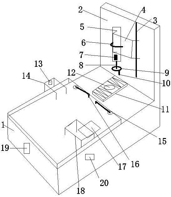
[0022] An intelligent wafer cutting machine tool, which includes a lathe body 1, a cutting frame 2, a slide rail 3, a lifting frame 4, a cutting arm 5, a fixing member 6, a motor 7, a transmission shaft 8, a wheel 9, a cutting tool 10, Workbench 11 , tray 12 , fan 13 , cleaning chamber 14 , first robot arm 15 , second robot arm 16 , storage table 17 , warehouse 18 , operating table 19 , and control module 20 .

[0023] One end of t...


PUM


Abstract

The invention relates to the field of mechanical cutting and specifically relates to an intelligent wafer cutting machine. The present invention provides the wafer cutting machine; an intelligent control module is adopted to control the machine, such that the cutting accuracy is improved; meanwhile, the modules and design of the cutting machine are optimized such that the cutting work is more effective. The intelligent control module is introduced in the intelligent wafer cutting machine to improve the cutting accuracy of the cutting machine; and the modules and design of the cutting machine are optimized such that the cutting work is more effective; as a result, the cutting success rate is increased and the production cost is reduced.

Description

technical field [0001] The invention relates to the field of mechanical cutting, in particular to an intelligent wafer cutting machine tool. Background technique [0002] Elemental silicon is a gray, brittle, tetravalent, non-metallic chemical element. 27.8% of the earth's crust is composed of silicon, second only to oxygen, and silicon is a relatively abundant element in nature. Silicon is found in quartz, agate, flint and common beach rocks. Silicon wafers, also known as wafers, are cut from silicon ingots. Millions of transistors can be etched on silicon wafers through special processes, and are widely used in the manufacture of integrated circuits. [0003] The manufacturing process of silicon wafers generally includes doping, melting, cutting, grinding, etching and cleaning. The growth of doped silicon ingots requires large blocks of pure polysilicon. These blocks, together with a small amount of special III and V elements, are placed on the quartz In Crucible, this ...

Claims


Application Information

Patent Timeline
Patent Type & Authority Applications(China)
IPC IPC(8): B28D5/02B28D7/00B28D7/04
CPCB28D5/023B28D5/0058B28D5/0082
Inventor 连新兰毛宝占
Owner HENAN GUANGDU SUPERHARD MATERIAL CO LTD
Why Eureka
Try Eureka