Silicon substrate suspended LED optical waveguide integrated photonic device and manufacturing method thereof

An LED device and integrated photonic technology, which is applied in the field of silicon substrate suspended LED optical waveguide integrated photonic device and its preparation, can solve the limitation of the development of nitride photonics and optical micro-electromechanical devices, immature nitride processing technology, difficult processing, etc. problems, to reduce the difficulty, improve the utilization efficiency, and simplify the production process.

Active Publication Date: 2016-03-30
NANJING UNIV OF POSTS & TELECOMM
View PDF9 Cites 22 Cited by
  • Summary
  • Abstract
  • Description
  • Claims
  • Application Information

AI Technical Summary

Problems solved by technology

However, SiC and sapphire substrates are not easy to process, and the processing technology of nitrides, especially

Method used


Image

  • Silicon substrate suspended LED optical waveguide integrated photonic device and manufacturing method thereof
  • Silicon substrate suspended LED optical waveguide integrated photonic device and manufacturing method thereof
  • Silicon substrate suspended LED optical waveguide integrated photonic device and manufacturing method thereof

Examples


Embodiment Construction

[0031] The present invention will be further described below in conjunction with embodiment and accompanying drawing.

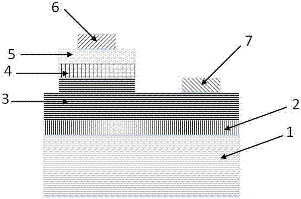
[0032] figure 1 , figure 2 A structural schematic diagram of the LED optical waveguide integrated photonic device with silicon substrate suspended in the present invention is given. The photonic device uses a silicon-based nitride wafer as a carrier, includes a silicon substrate layer 1, and an epitaxial buffer layer 2 arranged on the silicon substrate layer. The P-N junction arranged on the epitaxial buffer layer, the P-N junction includes an n-GaN layer 3, an InGaN / GaN quantum well 4 and a p-GaN layer 5 connected in sequence from bottom to top, and the p-GaN layer 5 is provided with The p-electrode 6 has a stepped mesa etched on the upper surface of the n-GaN layer 3, and the stepped mesa includes an upper mesa and a lower mesa on one side of the upper mesa, and the upper mesa is connected to the InGaN / The bottom surface of the GaN quantum well 4 is con...


PUM


Abstract

The invention provides a silicon substrate suspended LED optical waveguide integrated photonic device and a manufacturing method thereof. The device is designed based on the anisotropic silicon etching technique, wherein the silicon substrate layer and the epitaxial buffer layer of the device are stripped to be removed and then a suspended nitride thin-film LED light waveguide integrated photonic device is obtained. Furthermore, based on the nitride backside thinning and etching technique, an ultra-thin silicon substrate suspended LED optical waveguide integrated photonic device is obtained. In this way, the internal loss of the LED device is lowered, and the light extraction efficiency is improved. According to the technical scheme of the invention, a light source and a light waveguide are integrated on the same piece of wafer. Therefore, the integration problem of a planar photonic single chip can be solved. At the same time, the light emitted from the LED is transmitted along the light waveguide. As a result, the light transmission problem inside the light waveguide can be solved, and the plane transmission function of the light is realized.

Description

technical field [0001] The invention belongs to the field of information materials and devices, and relates to a silicon substrate suspended LED optical waveguide integrated photon device and its preparation technology. Background technique [0002] From a material point of view, nitride materials, especially GaN materials, have a high refractive index (~2.5), are transparent in visible light and near-infrared bands, and are excellent optical materials. However, SiC and sapphire substrates are not easy to process, and the processing technology of nitrides, especially GaN, is not mature, which limits the development of nitride photonics and optical micro-electromechanical devices. In recent years, by introducing AlN / AlGaN or other unique buffer layers to compensate for the residual stress caused by lattice mismatch and inconsistent thermal expansion, high-quality nitride materials based on silicon substrates have become increasingly mature and have gradually entered the marke...

Claims


Application Information

Patent Timeline
IPC IPC(8): G02B6/122G02B6/138G02B6/132G02B6/13
CPCG02B6/122G02B6/131G02B6/132G02B6/138H01L33/007H01L33/385G02F1/025H01L33/20G02B6/136G02B6/1223G02B6/1225G02B2006/12061
Inventor 王永进朱桂遐白丹许银朱洪波
Owner NANJING UNIV OF POSTS & TELECOMM
Why Eureka
Try Eureka