Method of manufacturing a semiconductor device

A technology for semiconductors and devices, applied in the field of manufacturing semiconductor devices, can solve problems such as increasing the size of memory cells, and achieve the effect of improving performance

Active Publication Date: 2016-03-30
RENESAS ELECTRONICS CORP
View PDF9 Cites 4 Cited by
  • Summary
  • Abstract
  • Description
  • Claims
  • Application Information

AI Technical Summary

Problems solved by technology

However, this increases the size of the memory cells, and thus a change to non-volatile memory that enables a reduction in the size of the memory cells is under consideration

Method used


Image

  • Method of manufacturing a semiconductor device
  • Method of manufacturing a semiconductor device
  • Method of manufacturing a semiconductor device

Examples


Embodiment 1

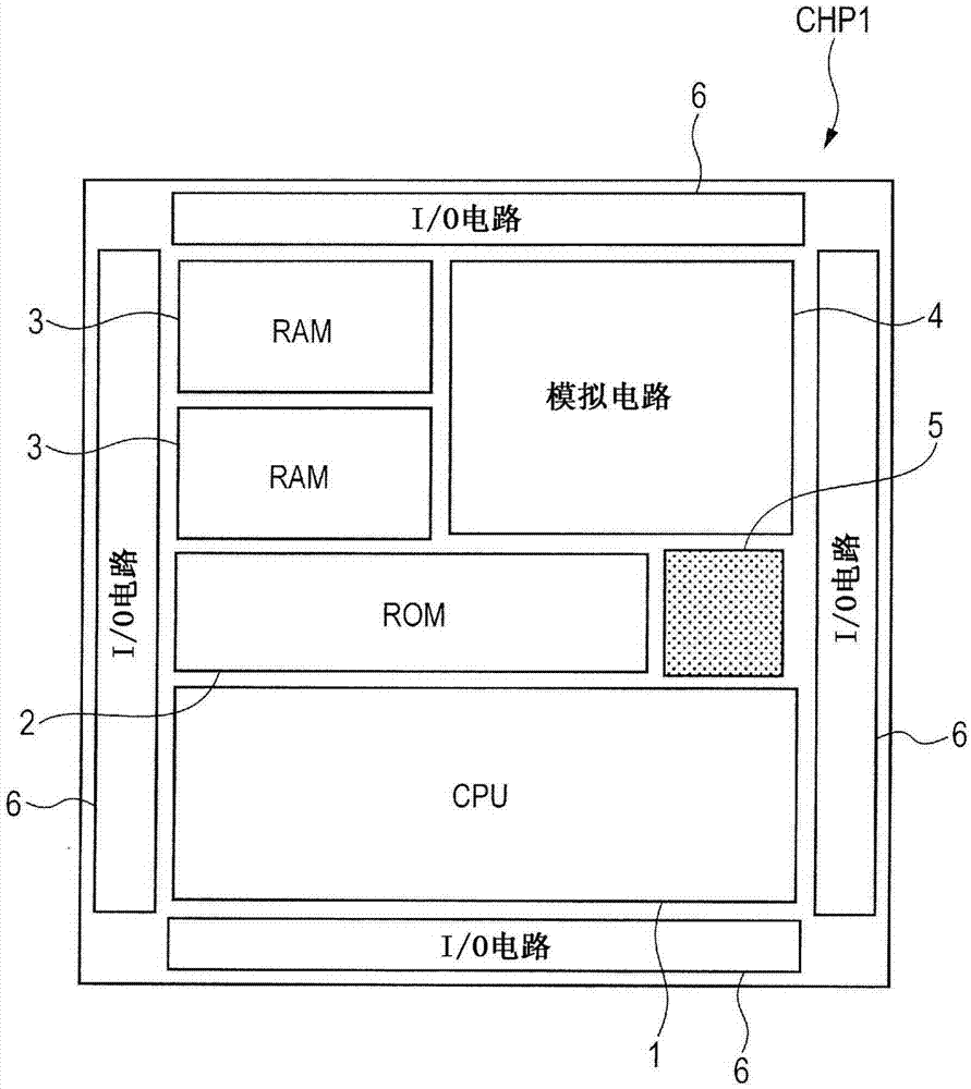
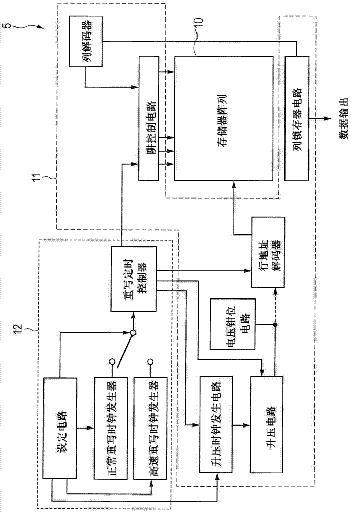
[0093] The technical idea in Embodiment 1 relates to a semiconductor device including, in the same semiconductor chip, a main circuit that provides the main functions of the semiconductor chip and a circuit that is added to the main circuit and is called an add-on circuit (add-on circuit). The additional circuit (additionalcircuit). In this semiconductor device, an attached circuit is formed of a MONOS rewritable nonvolatile memory.

[0094] For example, an SOC (System on Chip) includes a main circuit as shown below. That is, examples of the main circuit include: memory circuits such as DRAM (Dynamic Random Access Memory) or SRAM (Static Random Access Memory); logic circuits such as CPU (Central Processing Unit) or MPU (Micro Processing Unit); and mixed signal circuits including memory circuits and logic circuits.

[0095] On the other hand, examples of the auxiliary circuit include a storage circuit that stores relatively low-capacity information associated with the main ci...

Embodiment 2

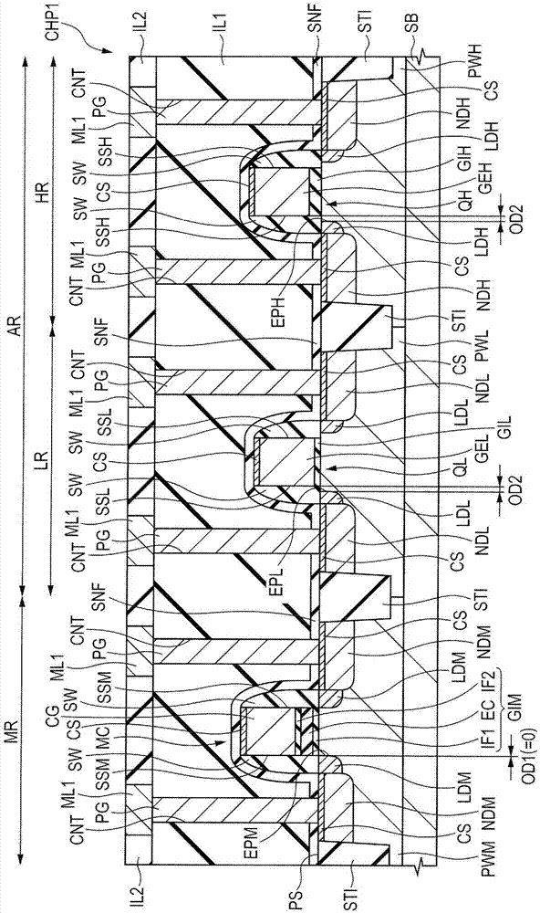
[0316] In the method of manufacturing the semiconductor device in Embodiment 1, in a state where the offset spacer OF2 is not formed on both side surfaces of the gate electrode CG, impurities are introduced into the semiconductor substrate SB to form n - type semiconductor region LDM. In contrast, in the method of manufacturing the semiconductor device in Embodiment 2, in which each has a thickness greater than that of each of the offset spacers OF2 is formed on both side surfaces of the gate electrode CG. In the state of offset spacer OF1, impurities are introduced into the semiconductor substrate SB to form n - type semiconductor region LDM.

[0317] It should be noted that also in Embodiment 2, the layout of semiconductor chips and circuit blocks in the nonvolatile memory may be the same as in Embodiment 1.

[0318]

[0319] Next, the structure of the semiconductor chip CHP1 as the semiconductor device in Embodiment 2 will be described with reference to the drawings. ...

Embodiment 3

[0370]In the method of manufacturing the semiconductor device in Embodiment 1, in the memory formation region MR, the insulating film IFG having the internal charge storage portion is patterned by dry etching. In contrast, in Example 3, the insulating film IFG having the internal charge storage portion was patterned by wet etching.

[0371] Note that the structure of the semiconductor device in Embodiment 3 is the same as that of the semiconductor device in Embodiment 1.

[0372]

[0373] Figure 57 is a process flowchart showing a part of the manufacturing process of the semiconductor device in Embodiment 3. Figure 58 to Figure 61 is a sectional view of the main part during the demanufacturing process of the semiconductor device in Embodiment 3. Figure 58 to Figure 61 A main part cross-sectional view of the memory formation region MR and the main circuit formation region AR is shown.

[0374] In the method of manufacturing the semiconductor device in Embodiment 3, in t...


PUM


Abstract

The invention relates to a method of manufacturing a semiconductor device. An improvement is achieved in the performance of a semiconductor device. Over a first insulating film formed over a main surface of a semiconductor substrate located in a memory formation region and having an internal charge storage portion and over a second insulating film formed over the main surface of the semiconductor substrate located in a main circuit formation region, a conductive film is formed. Then, in the memory formation region, the conductive film and the first insulating film are patterned to form a first gate electrode and a first gate insulating film while, in the main circuit formation region, the conductive film and the second insulating film are left. Then, in the main circuit formation region, the conductive film and the second insulating film are patterned to form a second gate electrode and a second gate insulating film.

Description

[0001] Related Application Cross Reference [0002] The disclosure of Japanese Patent Application No. 2014-193860 filed on September 24, 2014 including specification, drawings and abstract is incorporated herein by reference in its entirety. technical field [0003] The present invention relates to a manufacturing technique for a semiconductor device and, for example, such a technique that is effective when applied to manufacturing a semiconductor device in which a nonvolatile memory is embedded as a The attached circuit of the main circuit of the field effect transistor. Background technique [0004] In a semiconductor device formed with a main circuit including a MISFET (Metal Insulator Semiconductor Field Effect Transistor) as a field effect transistor, an additional circuit (subsidiary circuit) added to the main circuit can be formed separately from the main circuit providing the main function of the semiconductor device . Examples of additional circuitry include elec...

Claims


Application Information

Patent Timeline
Patent Type & Authority Applications(China)
IPC IPC(8): H01L21/8247
CPCH10B41/10H10B41/30H10B41/41H10B41/49
Inventor 大和田福夫篠原正昭丸山隆弘
Owner RENESAS ELECTRONICS CORP
Why Eureka
Try Eureka