Lateral double-diffusion field effect transistor and forming method therefor

A technology of lateral double-diffusion and field-effect transistors, which is applied in the direction of electrical components, circuits, semiconductor devices, etc., can solve the problems that the performance of lateral double-diffusion field-effect transistors needs to be improved, and achieves increased breakdown resistance, improved breakdown voltage, The effect of reducing dynamic loss

Active Publication Date: 2016-03-30
SEMICON MFG INT (SHANGHAI) CORP
View PDF3 Cites 7 Cited by
  • Summary
  • Abstract
  • Description
  • Claims
  • Application Information

AI Technical Summary

Problems solved by technology

[0004] However, the performance of the existing lateral doubl

Method used


Image

  • Lateral double-diffusion field effect transistor and forming method therefor
  • Lateral double-diffusion field effect transistor and forming method therefor
  • Lateral double-diffusion field effect transistor and forming method therefor

Examples


Embodiment Construction

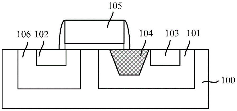
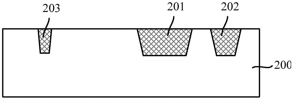
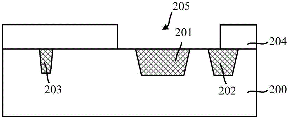
[0035] As mentioned in the background art, the performance of the existing lateral double-diffused field effect transistor still needs to be further improved. For example, the parameters to be improved include source-drain breakdown voltage, on-state resistance, gate-drain parasitic capacitance, and the like.

[0036] To this end, the present invention provides a lateral double-diffused field effect transistor and a method for forming the same. After forming the drift region, an inversion doped region is formed in the drift region, and the depth of the inversion doped region is less than that of the drift region. depth, the inversion doped region is doped with impurity ions of the first conductivity type, the drift region is doped with impurity ions of the second conductivity type, and the first conductivity type is opposite to the second conductivity type, so that the lateral double diffusion field effect The breakdown resistance of the tube increases, which increases the brea...


PUM


Abstract

The invention discloses a lateral double-diffusion field effect transistor and a forming method therefor. The lateral double-diffusion field effect transistor comprises a semiconductor substrate which is provided with foreign ions of a first conductive type in a doped manner; a first shallow trench isolation structure located in the semiconductor substrate; a drift region located in the semiconductor substrate, wherein the drift region surrounds the first shallow trench isolation structure and is provided with foreign ions of a second conductive type in a doped manner, and the second conductive type is different from the first conductive type; an inverted-type doping region located in the drift region, wherein the depth of the inverted-type doping region is less than the depth of the drift region, and the inverted-type doping region is provided with the foreign ions of the first conductive type in a doped manner; a body region which is located in the semiconductor substrate at one side of the drift region, and is provided with the foreign ions of the first conductive type in a doped manner; and a grid structure formed on the semiconductor substrate, wherein one end of the grid structure extends above the body region, and the other end of the grid structure stretches above the first shallow trench isolation structure. The grid-drain stray capacitance of the lateral double-diffusion field effect transistor is reduced.

Description

technical field [0001] The invention relates to the field of semiconductor manufacturing, in particular to a lateral double-diffusion field effect transistor and a forming method thereof. Background technique [0002] The power field effect transistor mainly includes two types: a vertical double-diffused field effect transistor (VDMOS, Vertical Double-Diffused MOSFET) and a lateral double-diffused field effect transistor (LDMOS, Lateral Double-Diffused MOSFET). Among them, compared with the vertical double diffused field effect transistor (VDMOS), the lateral double diffused field effect transistor (LDMOS) has many advantages, for example, the latter has better thermal stability and frequency stability, higher gain and durability stability, lower feedback capacitance and thermal resistance, as well as constant input impedance and simpler bias current circuitry. [0003] In the prior art, a conventional N-type lateral double-diffusion field effect transistor structure is as ...

Claims


Application Information

Patent Timeline
IPC IPC(8): H01L29/78H01L21/336H01L29/06
CPCH01L29/66659H01L29/7835H01L29/063H01L29/0847H01L29/1045H01L21/76229H01L29/0653H01L21/26586H01L21/76224
Inventor 郑大燮曹国豪
Owner SEMICON MFG INT (SHANGHAI) CORP
Why Eureka
Try Eureka