Detection method and structure for detecting trap states in GaN base heterostructure

A heterogeneous structure and detection method technology, applied in the direction of measuring electricity, measuring devices, measuring electrical variables, etc., can solve problems such as difficult to determine the spatial position of trap states, reduce the difficulty of test analysis, improve device reliability, and the method is simple and Quick and effective effect

Active Publication Date: 2016-04-06
北京中博芯半导体科技有限公司
View PDF6 Cites 11 Cited by
  • Summary
  • Abstract
  • Description
  • Claims
  • Application Information

AI Technical Summary

Problems solved by technology

However, because devices often contain multi-layer epitaxial thin film structures, each layer of epitaxial structure may contain trap states, and it is not very clear where the trap states really affect the device. Therefore, the above two methods are important in

Method used


Image

  • Detection method and structure for detecting trap states in GaN base heterostructure
  • Detection method and structure for detecting trap states in GaN base heterostructure
  • Detection method and structure for detecting trap states in GaN base heterostructure

Examples


Embodiment Construction

[0052] Below in conjunction with accompanying drawing, further describe the present invention through embodiment, but do not limit the scope of the present invention in any way.

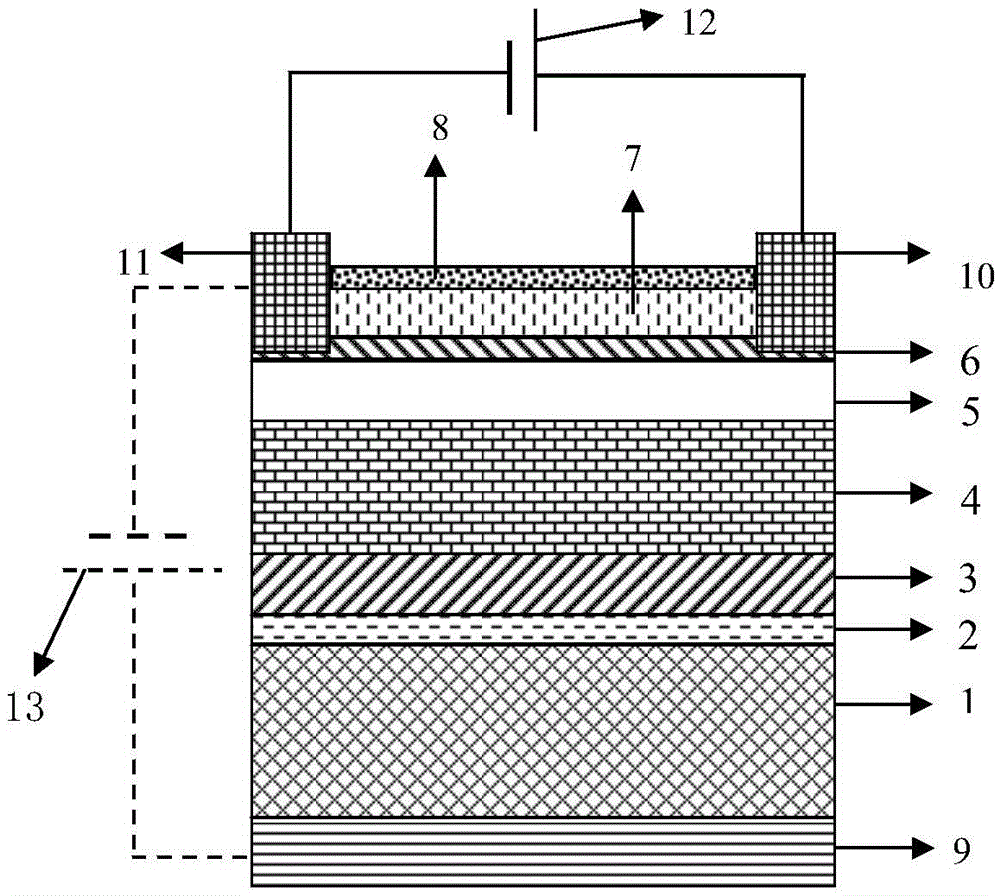
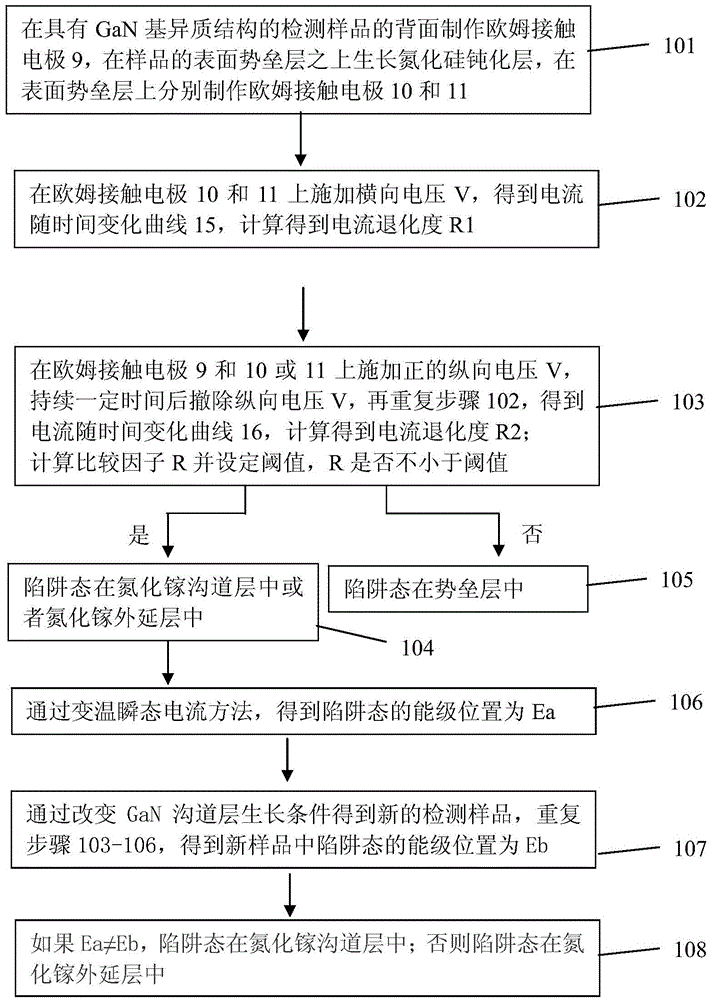
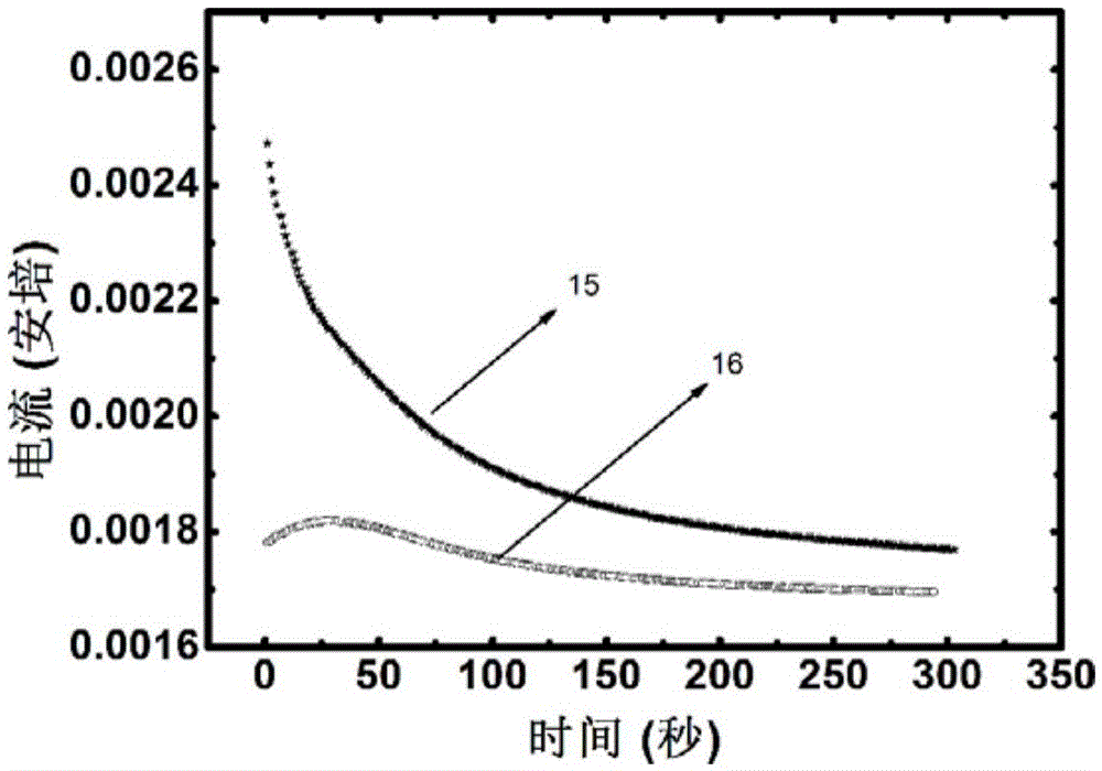
[0053] The invention provides a method for detecting trap states in gallium nitride (GaN)-based heterostructures. The GaN-based heterostructures on a conductive substrate are designed for the growth structure and test processing structure, and are formed on the surface of the sample and the back of the substrate. The three-terminal ohmic contact can study the capture and emission process of hot electrons under high field by applying longitudinal and transverse electrical stress, and then combine the sample structure design to finally determine the specific spatial position and specific type of the trap state in the sample, which not only reduces the It is difficult to test and analyze, and it improves the accuracy of identifying the spatial position of trap states, which can play an important role in ...


PUM

PropertyMeasurementUnit
Thicknessaaaaaaaaaa
Thicknessaaaaaaaaaa
Thicknessaaaaaaaaaa

Abstract

The invention discloses a detection method and structure for detecting trap states in gallium nitride base heterostructure. The detection method comprises the steps that the detection structure of trap states in the GaN base heterostructure is prepared; the trap states in the GaN base heterostructure is detected, conduction characteristics of a substrate and the sample surface are used for forming three-terminal ohmic contact on the sample surface and the substrate back, capture and ejection processes of hot electrons are studied by applying transverse and longitudinal electrical stress respectively; accordingly, whether the trap position in the sample is located on the GaN channel layer, or the GaN epitaxial layer, or the epitaxial layer is finally determined by changing the sample structure, and localization state information of the traps can be obtained. The method is simple, quick and effective, the trap states in the GaN base heterostructure can be determined, and the detection method and structure are good for further improvement of device reliability.

Description

technical field [0001] The invention belongs to the technical field of semiconductors, and relates to a detection method and a detection structure for detecting a trap state in a gallium nitride (GaN)-based heterostructure. Background technique [0002] The third-generation semiconductors represented by group III nitrides have excellent properties such as high band gap, high breakdown electric field, high saturation electron drift velocity, and strong polarization, especially based on silicon (Si) substrates and silicon carbide ( Aluminum gallium nitride / gallium nitride (AlGaN / GaN) heterostructure high mobility transistor (HEMT) on SiC substrate has excellent characteristics such as fast switching speed, low on-resistance, small device size, high temperature resistance, and energy saving. , is expected to be widely used in the field of next-generation high-efficiency and energy-saving power electronic devices, including microwave radio frequency power devices and power elect...

Claims


Application Information

Patent Timeline
IPC IPC(8): G01N27/00G01R31/26H01L29/06
CPCG01N27/00G01R31/2648G01R31/2831H01L29/0688
Inventor 杨学林沈波胡安琪郭磊程建朋张洁
Owner 北京中博芯半导体科技有限公司
Why Eureka
Try Eureka